return to main page

Weird loopy transistors
Causing Strange (loopy) voltage/current diagrams


NOT Weird Parts, but some fascinating bios


And - comments on a Berkeley press release

in 2005

Ron Williams and Bob Feretich currently find the failed logic cards in our 1401. They then replace the card (we have spares for most of the popular SMS cards in the processor) :-))
They then write up the defect as completely as practical down to the pin on the suspect SMS card.

Tim Coslet is the person who fixes most of our (1401 Restoration) defective SMS cards. His primary aid is an in-circuit tester that he built from plans in the magazine ???. The write up from the trouble shooters speeds his search for bad parts. Tim, using his in-circuit tester, can get a good idea of circuit dynamic characterists with out unsoldering the parts for individual testing - a good thing! (After a part is really suspect from the in-circuit test, it is removed for individual testing and replacement.) The source of the problem is usually:

  • an open diode (often cracked glass due to corrosion along the iron lead to glass interface)
  • a low beta transistor unable to adequately pull down a logic line
  • an open inductor
  • occasionally a somewhat shorted diode that causes excessive load on the drive element
Tim then replaces the defective part from components usually purchased locally, and verifies that the performance of the circuit is better - again using his in-circuit tester. He then marks the replaced part with a red dot - to show the replaced part, and returns the fixed SMS card to spares.


Using the in-circuit tester is not as straight forward as individual component testing - being an acquired art - but does speed diagnosis and reduces damage to parts and SMS card traces. :-))

(There have been thoughts of making SMS card testers and test programs. But with about 120 SMS card types and several circuits per card and several tests per circuit - this would be a non-trivial task.)
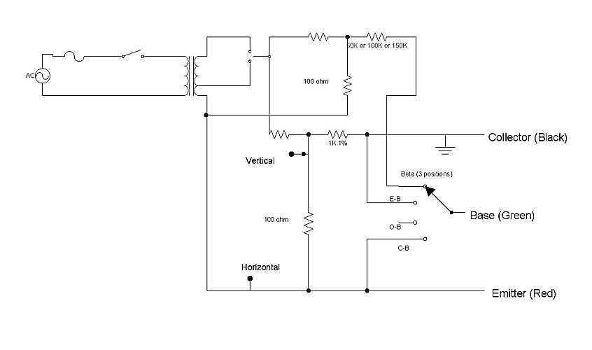
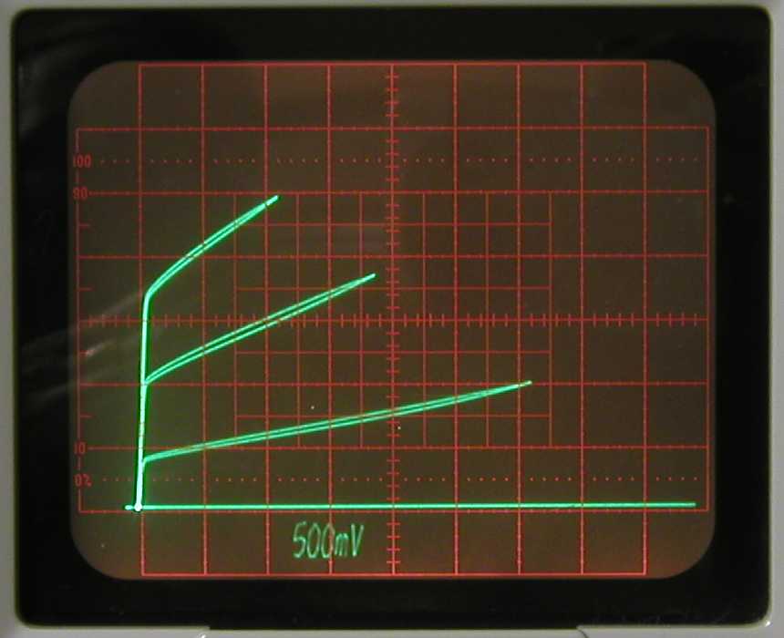
Tim's in-circuit tester
Notice on the left that the driving frequency is 60 Hertz, power line frequency - much lower than the service frequencies.
- Tim's test probes are marked "Collector (Black)" and "Emitter (Red)" in the diagram.
- The outputs from this circuit "Horizontal" and "Vertical"
are fed into the x and y axis of an oscilloscope that Tim brings with him.
And a switch selection of resistors can help determine if the beta (current gain) of a transistor is

- above or below 50
- above or below 100
- above or below 150

At the test frequencies and the resistances involved, the capacitors are practically open circuits and inductors are practically short circuits. These "reactive" components should not make phase changes (loops) in voltage vs. current curves at the much lower test frequency compared with the service frequencies.

A person expects straight lines from resistances, and sharply bent lines from transistors and diodes.

And on good boards, the above expectations are met - the expected patterns on the oscilloscope are actually seen. :-))

But the world is a strange place. Many of the circuits reported bad by Ron and Bob give very unexpected patterns.

Comments by Tim Coslet
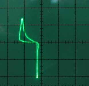
Looks like one of the Beta settings to me. The Beta of this transistor is close to the selected value, but it is leaking bad when reverse biased.
Looks like E-B to me.
Looks like C-B to me.
Looks like O-B to me.

We are at a loss to explain these loops. (Thermal effects seems unlikely to provide this level of change??) Please send suggestions to Ed Thelen ed@ed-thelen.org and Tim Coslet

Added Feb 23, 2006


Further details by Tim Coslet - Feb 23, 2006

The original design in the magazine used +-1V peak to avoid possible damage to semiconductors during in circuit test, but this is too small to turn on darlington transistor E-B junctions so I increased my design to +-2V. I also added a +-10V peak range to check reverse breakdown, low voltage zeners, and operate transistors at higher voltages. All the 1401 testing has been done on the +-10V range, as this seemed more "realistic" to me and I was having problems getting good Beta estimates on the +-2V range (due to an effect mentioned below almost all the transistors read very low Beta on that range, but more normal Beta on the +-10V range).

The scope was not set to 1V/div. I usually use 0.5V/div when using the +-2V range and 2V/div when using the +-10V range (so the curve fits the screen better). Unless I need to determine transistor type (Si/Ge) or breakdown voltages I'm more concerned with shape than exact voltage/current levels.

E-B is the Emitter-Base junction with the Collector shorted to Base.
O-B is from Emitter to Collector with the Base not connected (open).
C-B is the Collector-Base junction with the Emitter shorted to Base.

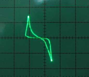
These are standard test definitions given in datasheets that I wired into my switch, so that I would not have to keep swapping leads around.

The Beta settings use an additional similar resistor network to inject current thorough the Emitter-Base junction while the main circuit is measuring the characteristics of the Emitter to Collector path (similar to the O-B measurement, but with the Base connected instead of open). The difference in the additional similar network is that the 1K resistor is replaced by a Beta*1K resistor (50K, 100K, and 150K in my box) and there are no scope connections to that circuit. To a first approximation, if the resistor selected exactly matches the Beta of the transistor then the curve drawn will be identical to the curve drawn in E-B mode, if the resistor selected is larger than the Beta of the transistor the curve drawn falls outward, if the resistor selected is smaller than the Beta of the transistor the curve drawn pulls inward. However this is never exact as the test circuit has no compensation for the E-B diode characteristics (a second approximation effect that changes between transistor types) and the curve sometimes begins falling outward then pulls inward.

A transistor on this tester should NEVER give any loops on any setting and the transistors on these cards are the first time I have encountered this! It means, for some reason, the transistor is stopping conduction far differently than it starts conduction. My suspicion is a thermal effect as I have seen many of the loops change size/shape the longer I leave the transistor on the tester.

I believe you took all those photos on one transistor.

--

R. Tim Coslet
(for e-mail address, go to Team Bois)


March 1 update from Robert Garner
Ron, Tim,

They're real: I've confirmed Tim's loopy/hysteresis I-V transistor curves on a Tek 7CT1N curve tracer plugin in my 7834 scope.

The 1st four traces are for NPN 083, bad sample #1, where horizontal collector voltage is about 2V/div, vertical collector current is 0.2 mA/div, and base step voltage amplitude is 10mV/step.
First screen pic is six base steps,
2nd one is single base voltage,
3rd one is eight,
4th is four base voltages (with these last two at 1mA/div collector current and 50mV and 100mV per steps, respectively).
Next two screen pics are 083, bad sample #2.
083-2,v=2V_div,i=1mA_divFour100mV
083-2,v=2V_div,i=1mA_divOne
And last screen pic is a good, "new old stock" NPN 2N1302, but at lower 20mV per base step.
Shows this new transistor has much better (~5x) beta than the loopy ones. (But I do see tiny loops in the higher base voltage traces too.)
Traces were rock solid and didn't move or change over time.

Any explanations?

(Mysterious ferromagnetic effect instigated by iron diffusion from wire leads into junction? ;-)

- Robert

Rick Dill's comments on "Loopy Transistors" - added July 2009
Robert Garner says Rick was later an IBM Fellow
The 1401 transistors were germanium, although at the end of the SMS days, silicon transistors were found that could be used as substitutes in most cases or at least replacement boards were made with silicon transistors that were voltage and signal level compatible.

The mode of loopy behavior in the silicon mesa transistors is similar to germanium. Mesa transistors had the collector diffused into the silicon over the entire wafer. The emitter was produced by a second diffusion or an alloy process (micro-epitaxy) and the emitter and base connections were covered with wax (or later photoresist) and were protected from an etch which went through the collector junction leaving the emitter and base on a tiny mesa of silicon. These junctions had no oxide protection except for the extremely thin native oxide and were sensitive to surface contamination as were the germanium emitter and collector junctions. The cans that transistors were put in or the plastic encapsulation of low cost transistors were to provide a hermetic seal and protect the sensitive collector junction. Contamination inside the can or any leaks resulted in leaky transistors.

The experimental tools we had were primitive compared to those even a few years later when we came first to really understand silicon junction passivation by oxides and through that to have some affirmation of what was deduced from primitive experiments for unprotected silicon and germanium junctions. There were some very early lessons from the solid logic technology (SLT) planar transistors used for the IBM 360. The theory of that design was that the transistors were protected by a low temperature powdered glass layer put onto the surface and then melted to give a hermetic seal to the junctions. This in theory would stabilize the transistors, but the theory didn't work because sodium atoms in the SiO2 layer lying under the frit glass layer were mobile ... unless the transistors had that locked up in a phosphosilicate glass layer from the emitter on NPN transistors. PNP transistors didn't have problems with surface inversion and were stable without the psg layer. That really didn't come out in technical publications until the advent of field effect transistors where the role of sodium in the SiO2 layer was a major issue in controlling both leakage and threshold voltage. IBM used PSG, while Intel and others essentially eliminated sodium by lots of washing before any thermal cycle which could lock fingerprints or other sodium contamination oxides.


an abstract with images
From the abstract, the article seems to be the first salvo in the common wisdom that "Cu is evil around Si"?:

(a) In the presence of bare copper in an oxygen free ambient, power aging degrades the emitter parameters and gain. Only partial recovery can be achieved by etching into the bulk silicon or by heating the device at 300�C (bulk failure). (b) In gold plated and/or oxygen backfilled cans, soft, loopy reverse junction characteristics develop under both temperature and power agings, first on the collector and later on the emitter. Both junctions. recover completely upon opening the can and drying the transistor surface (surface failure). Surface failure is caused by water adsorption over the surface of the silicon wafer. Experimental evidence, including aging experiments in atomic hydrogen, is presented to demonstrate that the bulk failure is caused by copper contamination in the bulk silicon. Copper is transferred from the can to the wafer via a volatile hydride. It diffuses into the silicon and becomes electrically active during power aging. Qualitative explanations are offered for both failure modes. Surface failure is due to surface states introduced by the adsorbed water and/or ionic conduction. In order to explain bulk failure, the solubility and precipitation of copper is examined over the transistor profile and the effect of field on the migration of copper in silicon is taken into account.

Some of their loopy curves:

Lectures on Memristors, Dr. Chua added Feb 13, 2016
Here is a series of lectures by Professor Leon Chua. And from Wikipedia.
Warning: If life is comfortable and you don't want to churn up your brain, avoid this stuff ;-))

Dill to Garner - Re: Alloy Transistors - 09/03/2008
From: Rick Dill
To: Robert B Garner/Almaden/IBM@IBMUS,
Date: 09/03/2008 10:14 AM
Subject: Alloy Transistors

Robert,

The early 1950's were an interesting time. In the summer of 1951, Bell Labs had a "summer school" for a fair sized group of university professors. The professor who taught optics attended and had lectures from the likes of Shockley and Bardeen as well as some laboratory hands on time. They published a paper with everyone as an author in which they confirmed the Einstein Relationship between drift of electrons and holes under electric field and thermal diffusion. They returned to campus with a small kit of experiments which a fellow student, Jim Boyden and I latched onto and used both for recreation and every opportunity for a project. We were sophomores when we got our hands on this.

It included a germanium alloy diode for measuring IV curves, a chip of germanium with rhodium plating on the back (which we had to learn how to replace after etching it off) to be used for making point contact transistors, and a bar of germanium for the Shockley Hall measurement of drift and diffusion of electrons. We fabricated our own point contacts and crude manipulators to put them down near where we wanted them.

In the summer of 1954. fresh with a B.S. in physics I had a job at IBM in Poughkeepsie. It was my first industrial research experience and a wonderful experience. Joe Logue was the manager of the small group which included Hannon York, the engineer who invented the current switch circuit (non-saturating), Bob Henle who was a really good circuit guy and lead the company a few years later to abandon core memories and go to semiconductor memories.

At the time, the group was just off of the CRT based electrostatic memories used in the 701 and the later mica target CRT-like memories used in the following computers up to the introduction of magnetic cores which were just coming visible in 1954.

My assignment was really a gift. Joe wanted higher function circuits with the example being the neon ring counter. As he has told you, with no real hands on experience I was able to postulate that we might be able to produce such a thing with a double-based diode (unijunction transistor) which had multiple emitters and with the help of the small group in the pickle factory actually get a four-state device prototyped. Dick Rutz and John Marinace were the key people in that group and I eventually ended up working for in Rutz's group.

I also postulated an adder circuit based upon the Shockley Hall structure, but with deflectors to steer the electron cloud sideways to multiple collectors. We didn't make this, but it did show up a decade later as an academic achievement.

While Bell Labs was stuck on point contact transistors (and even made a computer out of them), Joe Logue has recognized the superiority of junction transistors. From a circuit standpoint, the ones available had too much base resistance to work well in digital circuits, although this didn't hamper them for communications. He tried to encourage the vendors to make transistors with low base resistance to little avail since computers were not important to the electronics world at that time.

The task got handed to Research where on the fabrication side the team of Rutz and Marinace and their technicians made alloy transistors with a small alloy emitter surrounded by a circular base contact, and a larger collector junction on the back side of the die. Contrary to what most people believed, alloying was a well determined metallurgical process when done right.

To do it right, you needed the crystal to have a <111> orientation. This is the slow dissolving direction when subject to dissolution by molten metal, so the sides of the dissolved region were angled along <111> planes and the bottom flat. The depth depended on the volume of the alloy "dot" and the temperature. On cooling, the germanium first cleanly regrew precipitated from the melt and was doped by the materials in the dot (indium gallium for PNP transistors and tin antimony for NPN). The collector on the backside was simply larger and etched more deeply into the germanium chip.

The design was IBM's, but we went to TI and contracted with them to manufacture germanium transistors for us. We were allowed only to make 10% of what we needed, which gave us room for special applications such as core drivers or advanced devices before releasing them to TI.

In spite of Joe Logue trying to get me to stay and do graduate work in the Syracuse MS program, I went back to Carnegie Tech and moved from physics to EE. 18 months after that Bob Henle visited campus following up on a summer job one of the young faculty had a year after me. IBM wrote three separate contracts. One supported my research with the requirement that I come to Poughkeepsie roughly monthly to report on my progress. The other two supported Dale Critchlow, the young faculty member, and Bob Dennard, one of his students. Both Dale and Bob were working in magnetics at the time. I was the first to join IBM in February 1958 and Critchlow and Dennard joined the following summer. We were all in the same group trying to do circuits with multi-hole magnetics and transistors. I left that project in summer of 1958 to go to Poughkeepsie and work for Dick Rutz with my initial assignment being to duplicate Esaki's work in Japan on tunnel diodes.

In 1955, I worked at RCA Labs for the summer on silicon diodes and the observation that they did not behave according to Shockley's theory. There I met Herb Kroemer who is credited (among other things) as the father of the "drift transistor". Kroemer postulated (as a theorist) that a graded impurity doping in the base region would provide a field that greatly speed up transistors. It was only after I got to IBM that I read a patent of Lloyd Hunter which is the patent on the structure, so IBM has at least as much claim as RCA. By diffusing (probably phosphorus) into the germanium blanks, the IBM design became much faster.

In 1958 on returning to IBM, I found that the development group had built a fully automated factory for producing alloy transistors. It used syntron sonic driven bowls to feed to germanium die, alloy spheres for emitter and collector, stub leads soldered to the spheres during alloying, and the dished base contact washer. These were fed into high purity carbon fixtures, one for each transistor. Once the assembly was together it went through a hydrogen furnace, after which the transistor was extracted, etched, washed, dried, tested, and then assembled onto a header. The carbon fixture was sent back to be re-used. This room-sized automated factory could product 40 million transistors a year, which was more than IBM needed. We shipped the factory to TI with the stipulation that they could use it only for IBM production for a stated number of years.

When the diffused base transistor came in, it was only a small modification to the line to get the die right-side-up so that the diffused surface was facing the emitter.

About 1964 I visited TI and saw multiples of this production facility running full tilt to make germanium transistors for the world.

Silicon really came in with the system 360. The group that met to work out what would be done was the Compact Committee. I was a research rep on that team. We should talk about that sometime. Bill Harding was one of the key people and I believe that he is still around in Southern CA. What became solid logic technology (SLT) came from his declaration that he could produce individual transistors very cheaply and solder them directly to substrates. This was all an act of faith, but it came to fruition and significantly delayed IBM's serious entry into integrated circuits for logic.

When we did get into integrated circuits for logic, electron beam lithography played an immense role in giving IBM a competitive advantage. Hans Pfeiffer was the leader in this technology and is now in Carmel Valley.

This is just a little background for out Thursday discussion.

Rick

Dill to Garner - Re: Science behind loopy transistors - 12/08/2009
Rick Dill
12/08/2009 09:33 PM
To: Robert B Garner/Almaden/IBM@IBMUS
cc
Subject: Science behind loopy transistors

Robert,

The article by Montgomery and Brown is probably as good a reference as you will get given the understanding at the time. It is very crude experimentation with the use of a strontium titanate dielectric coupled to the semiconductor by simple mechanical contact is laughable today. Still, it does find that surface accumulation, surface depletion, and surface inversion on p-type samples which varies depending upon the ambient. It was done on high resistivity samples in order to see any significant penetration of a space charge layer into the bulk.

On the other hand, the uneven gap between the dielectric and the semiconductor makes the whole thing very crude. A thin film dielectric on the surface is what is really needed to look at this phenomenon, something we didn't do until we got to silicon and then went back to with germanium. There MOS capacitance measurements can give you a good idea of the charge in the dielectric and with FETs can give you a direct measurement of the surface mobility under various conditions. Transient MOS capacitance allows you to see the recombination. But in the 1950s you didn't have those tools. I wrote a couple of the earliest papers on applications of semiconductor capacitance (voltage dependent) in 1956 and 1957. When I was playing with automated measurements in the 1970's we did automated MOS measurements including all the fun transient stuff that was new science then. We designed a mercury probe that let you make contact to a dielectric surface without having to evaporate and pattern metal. All fun and done with summer student and only ended up in internal reports.

One can draw from the paper that the transistors with the biggest issues would be the npn with moisture causing a surface inversion surrounding the collector that would gobble up holes injected into the base(along with the collector, of course) and both lower the breakdown voltage at higher currents and also induce a time when they has to be drained out via a resistive path to shut off the transistor.

Do we see the loopy behavior in both npn or pnp transistors. I suspect that it is most common in the former.

On pnp transistors, one might expect to see the breakdown decrease with a wet ambient.

There are lots of papers out there which tried various treatments and observed current gain and sometimes loopy behavior, but they weren't getting at the root cause.

The big issue here is that surfaces can change charge (i.e. ionics in surface films) and this can either accumulate or invert the surface .. or sometimes the best case of leaving the bands essentially flat.

Surface states and surface recombination come into play because on a surface moving toward inversion, there will be an electric field helping the minority carriers get there. This will show up as small differences in current gain.

Not sure this makes sense, but the one sentence answer is:

Reference 16 is about as good as you will get without some immense amount of searching.

Rick

It agonizes over surface states, which are probably much more important in terms of recombination and the frequency dependence than in transport of carriers.

Dill to Garner - Re: Science behind loopy transistors - 12/09/2009
From: Rick Dill
To: Robert B Garner/Almaden/IBM@IBMUS,
Date: 12/09/2009 09:35 PM
Subject: Re: Science behind loopy transistors

Robert,
In the late 1940's we had the Shockley "Electrons and Holes in Semiconductors" which pulled together the basic physics of motion of electrons and holes under equilibrium and non-equilibrium conditions. It only crudely handled the "forbidden" transition that caused electrons and holes to combine, behind the lifetime of minority carriers.

This let us understand diodes, junction transistors, and Shockley's purely theoretical junction transistor (closest to the jfet today). It described the forward and reverse current voltage curve of germanium diodes very well with the relationship

       I =I0 eqv/kt

Lifetime was buried in the I0 with a whole lot of hand waving and studies which identified surfaces as bad actors and talked a lot about surface states and the like.

This was the physics I had when I did my PhD and the thing I never could handle was lifetime. It was a constant I could put into my equations, but I had no idea how to assign values to it.

I also became aware in my 1956 summer job working for Paul Rappaport at RCA Labs that this theory didn't work for silicon diodes. The kt term became nkt where n was typically something like 2. My assignment was to make silicon diodes and measure their current voltage curves. This was one of the topics I proposed as a thesis topic, but rejected it because I didn't have a clue how to answer the question. A classic paper by Shockley, Noyce, and Sah answered that.

Surface effects were largely not well understood, but the rather crude experiments in the paper you cite give a clue (largely missed).

Other clues came from experiments and procedures to control base-collector breakdown. The breakdown is reduced by the geometric effects of junction curvature near the surface and also by any surface accumulation which thins the junction at the surface causing early breakdown. If the surface is depleted or inverted, the breakdown isn't affected, but the junction leakage can be high. All of this is well beyond the one dimensional theories of Shockley.

Once the surface is inverted (by almost anything), then loopy behavior becomes possible. In silicon the big culprit was human sweat. Sodium on the surface (NaCl) would have the sodium incorporated in the oxide. This ion would move with field and when close to the surface would induce mirror charge in the semiconductor playing havoc with things like threshold voltage of FET transistors. Once we understood those phenomenon, the germanium story because a whole lot more understandable .. except that no one cared any more.

That's it for tonight.

Rick

Meyerson to Garner - Re: Loopy I-V curves in 1950s Ge alloy-junction transistors - 04/23/2014
From: Bernard S Meyerson/Watson/IBM
To: Robert B Garner/Almaden/IBM@IBMUS, Gary Patton/Fishkill/IBM@IBMUS, Pmooney@SFU.CA
Cc: ....
Date: 04/23/2014 05:06 AM
Subject: Re: Loopy I-V curves in 1950s Ge alloy-junction transistors (from our IBM 1401s at the Computer History Museum)

Robert,
     My bet is that this originates from deep traps in the materials. At that time there was nowhere near the controls needed to prevent chemical contamination from myriad sources, and as such the traps relaxation times are what is being seen in the IV curves. What gives me reasonable confidence is that when you illuminate the transistor it suppresses the phenomena, indicating that an excess of carriers backfills states. The best way to do this is to have someone do DLTS on a dot or even a surface point contact, and Patricia Mooney might be the best person for the task. Last I heard Pat is in Simon Frasier University, I suggest you contact her and explore her having an explicit look at this. Her website is below. I also copied Gary Patton who once upon a time knew about things like transistors:-) Gary, what say you on this one?

Best Regards, Bernie

http://www.physics.sfu.ca/people/profiles/pmooney

From the Desk of;
Dr. Bernard S. Meyerson, IBM Fellow
VP, Innovation
IBM Corporate Headquarters
1101 Kitchawan Rd.
PO Box 218
Yorktown Heights, NY 10598
Ph: (914)-945-2206
Fax:(914)-945-4245
Email: Meyerson@US.IBM.COM

Dill to Garner - 03/26/2016
From: Rick Dill
To: Robert B Garner/Almaden/IBM@IBMUS
Cc: Constantin Bulucea
Date: 03/26/2016 09:07 PM
Subject: Re: Fw: Seeking semiconductor physicist to explain Loopy I-V curves in old Ge alloy-junction transistors (from our operational IBM 1401s at the Computer History Museum)

I don't think that deep traps are the issue here. This was a bogeyman explanation for all sorts of problems associated with copper/gold/and-other contaminants in germanium. The ease is making germanium transistors was inadvertantly helped by the "alloy junction" process because these highly mobile materials were gettered out of the germanium into the molten metal. I (perhaps stupidly) used copper plated contacts on the unijunction transistors for my PhD work. They should have killed the lifetime in the germanium bars, needed by the device. I'm pretty sure that the copper in the germanium was gettered out. On the other hand Myerson has much more recent experience with germanium and he needs to be paid attention to.

More likely, the funny loops were a function of the transistor bias cycles and surface inversion layers (which we didn't understand at all except that good clean-up etches got us good junction properties). In forward bias, these inversion layers would be well connected to the emitter and would also inject carriers into the base region (both near the narrow base junction and also outside). Turning off the emitter probably disconnected the surface inversion layer from the emitter. The excess carriers in the base (Ge has long carrier lifetime) and they would drift to the collector continuing the collector current until they were all collected or died due to lifetime.

If you made transistors and etched their surfaces to a "clean" state and then encapsulated them in a can, they didn't get the moisture and "whatever" to form the inversion layers. If, on the other hand, either the solder seal of the can leaked or the iron in the leads rusted out, they would not be kept "dry".

We need someone who learned from inversion layers in silicon, which became well understood some years later, to look at the funny curves and their temporal and optical behavior.

I have been looking for a message verifying a time that Constantin and I might get together with you to talk about this. We started in February with a decision that Wednesdays might work. I hear nothing after my reply as to when I was available.

Rick

Dill to Garner - 03/28/2016 - More on Loopy Transistors
More on Loopy Transistors

Rick Dill
3/28/2016

Just Plain Alloy Transistors – IBM Style

The 1401 came before we were doing diffusion of impurities into semiconductors. That came a little later. These were made on wafers aligned crystalographically with the surface being a <111> face. This is the slow dissolving face with many etches and also with the metals used for the emitter and collector alloy. The alloying is a crystalographic micro-etching by the metal "dots" used for emitter and collector. This gave a near-crystalographic flat bottom to the extent of the melting. The initial steps of the cooling were a recrystalization heavily doped with the appropriate impurity (gallium for pnp and probably antimony for npn). As the cooling proceeded rapidly, the melt became a mix of metal and polycrystaline germanium, getting more metallic toward the surface.

This alloying was a low temperature process done in a reducing atmosphere to help get wetting. The "clean-up" etches used afterwards were to both etch the metal back a little because it may have spread out over the base surface where there had been no alloying and also to get the surface back to an appropriate condition so that the transistor leakage at the surface was low.

The wafers were diamond cut from an oriented crystal, then mechanically polished and etched with an anisotropic etch to remove about a micron or so of lapping damage. It was fairly deep in germanium which is mechanically weaker than silicon. In the late 1960's we would have used a chemical-mechanical polish instead which was (if I remember right) a sodium hypochorite solution and a non-woven fabric pad, without any abrasive.

My frail memory cannot remember the etchants used and I haven't uncovered my PhD thesis which probably had some of the formulations in it. It hasn't been unpacked since it got moved to California a decade ago.

These wafers were then ultrasonically cut up to make round chips of controlled thickness. The polishing was probably developed by Earle Harden, a toolmaker with very skilled fingers for creating small transistors and a love for precision machining through lapping.. I first worked with him as one of my teachers and then was his manager for some years where I utilized his skills in many ways.

After he left me, he joined David Thmpson on the project that made the first thin first thin film magnetic recording heads. Earle pretty uch defined the diamond lapping process for the air bearing surface that isstill used today. I had a small role in that project. David,Luby Romankiw and I kicked over the idea of using lithography and thin films for recording heads. I had the ability to quickly make masks using the fly's eye lens which gave me a 2 micron or so capability on-axis degrading from spherical aberration. Knowing the limits and with a decision on the number of turns, I designed the masks and cut them in rubylith at 500x, so I might claim to be the designer. I made the masks after hours since it wasn't part of my day job.

The wafers were relatively lightly doped in order to get the high ration of carrier concentration between emitter and base. This was of course a compromise between current gain and base resistance. It was also the reason for the ring washer base contact. In essence, these transistors were different from any silicon bipolar transistors which always had fairly high surface concentrations surrounding the emitter which naturally came from the double diffused emitter/base and helped suppress the emission at the edges of the emitter. It also made the surface of the junction less sensitive to surface inversion.

So we have a lightly doped base region. I don't know what etchants were used, but the final etch and blow dry would be intended to leave the surface in a low leakage state at both emitter and collector. The reason for the glass metal lead header and soldered cap was to hermetically seal the transistor in an environment where it wouldn't be subject to changing moisture and other contaminants. It worked remarkably well for many years.

I believe that all the "loopy" transistors we are looking at are ones which have surface contamination. While Pat Mooney is a good reference for deep level traps in semiconductors, including germanium, I don't think that is the big issue here. As I recall, Pat came to IBM and worked toward the end of the mid 1960's germanium program looking at deep traps, although we never got to long term passivation for that because silicon was close enough to Ge in speed at that time, that you wouldn't go backward for the 1.e to 2 times we eventually understood as its superiority, at least at that time. Its time may come, though.

The etchant would presumable leave the surface in some sort of condition that we didn't come to properly appreciate until we made surface devices in silicon. There, with silicon oxide structures (MOS) we learned about flat band voltages and about charge creating electric fields at or above the surface. That all came in in the early 1970's.

I got to go back to my roots in semiconductor capacitance again with MOS as I had with junction capacitance. None of the MOS work was published because my real focus was on automated measurements and lithography, but it gave Thomas Garwin, a summer student, a great experience while he was deciding whether to do physics or history. He went to Harvard and did history (of science).

I believe that Hwa Yu at IBM did some work on germanium FET devices after the bipolar program. I really didn't ever talk to him much about that because his boss thought I was a traitor to kill the bipolar program I'd started when we discovered a flaw in the underlying assumptions of superiority to silicon. The problem was the limiting velocity of electrons in germanium (similar but not as abrupt as what causes Gunn Effect in GaAs).

Let me assume that the surfaces were near flat band. They would be relatively easy to move away from that if there was ionic charge at or near the surface. The light doping would make it relatively easy to either get an accumulated surface or the alternate of a depleted or inverted surface.

Since we had both npn and pnp transistors, I would expect changes due to the environment to be different for the two types of transistors, so we need to look for differences between the two and see if we can explain both phenomenon.

Let's look at the parameters. There are voltage breakdown and thermal effects on leakage. There are effects from either surface charge depletion or inversion layers. I believe that there were some papers on inversion layers and transistor turn-off, but I don't remember the terms we might have used to described them before we understood MOS.

OK .. a thought!!! You might be able to get some MOS measurements if you could take a small anodized aluminum or titanium film spot as one electrode and place it on the base surface and do a MOS capacitance measurement. It would need a soft backing to get good contact without changing the surface much. Might be too invasive.

We need to think through the effect of an accumulated, depleted, or inverted surface on transistor behavior. That includes the emitter being expanded by an inversion layer which would become more conductive and inject carriers during forward bias of the EB junction. When the transistor is turned off, the inversion layer might be partly or fully cut off from the inversion leaving the inversion still emitting. This would also be a region of the transistor where the carriers take longer to get to the collector. I believe this explanation is in the literature, but don't know where to find it. It may only have been an oral paper and never published on paper.

On the other side you need to look at what a strongly inverted surface would so and whether it would affect breakdown, Particularly you might need to understand this as perhaps having a thermal sensitivity.

Finally, you need to look at the effect of saturation in the transistor. This is another circuit effect that is essentially loopy. It takes a while for the transistor to shut off. I believe that all the 1401 circuits are saturating and that there is emission into the bulk regions of the base that take time to clean out either by lifetime or carriers getting to the collector as its voltage rises.

Lots of this stuff changed a lot when we went to diffusion and epitaxial base layers with a base diffusion to lower base resistance, much less space between emitter and base contacts. And diffused emitters. At that point the impurity concentrations at the semiconductor surface were much higher.

We can learn about that era when we decide to restore one of the few Stretch or 7090 machines. Those transistors were very much like the 1401, but they had a diffused base (speeding carriers across because of its impurity gradient) and much higher impurity concentration of the base surface, even though they were structurally very similar to the 1401 transistors.

The post-alloy diffused transistors we and TI worked on in the mid 1960's were real planar structure transistors and had dimensions from lithography in the 2.5 micron range. TI was interested in low noise from low base resistance and we were interested in maximum switching speed.

Meeting with Rick Dill, Constantin Bulucea, and team Mar 30 2016
Robert Garner organized a meeting to discuss Loopy Transistors.
Present were
     - Rick Dill - expert witness, also taught transistors to Constantin at Berkeley
     - Constantin Bulucea - expert witness
     - Robert Garner
     - Ron Crane
     - Bill Newman
     - Ed Thelen - an unbeliever - no filament, can't work ;-))

We gathered about 11:30, and it soon became evident that hand waving was not doing it - enter the white board - the engineer's mouth piece.
left to right, Bill Newman (who had provided much of the photographic evidence), Rick Dill, Constantin Bulucea
About 12:30, the rest of the resortation/maintence crew came to eat their lunches.
Note the photos of the evidence on the projection screen.
Here Robert Garner is ... I didn't understand ;-)) The technical discussions continued until about 1:30 when business pressures called some away.

It was evident that more evidence and more test conditions were needed. At the next gathering Robert will bring his specialized 'scope, more transistors, and a test setup with more options.

This picture, of Professor Rick in full voice, was taken by Constantin.
Note that the diagrams have shakey "doping" boundaries, and there are no equations to threaten and intimidate "the rest of us" ;-))


In preparation for the April, 6th meeting, Robert prepared 12 photographs of I/V curves.
This one is as confusing as any. Hint - there are not supposed to be any loops present, just curves.

Meeting with Rick Dill, Constantin Bulucea, and a group April 6, 2016
Robert Garner organized a 2nd meeting to discuss Loopy Transistors.
Present were
     - Rick Dill
     - Constantin Bulucea
     - Robert Garner
     - Ron Crane
     - Bill Newman
     - Ed Thelen
     - Marc Verdiell

The group gathered in the CHM 1401 Workshop at 11:00 to watch Robert Garner demo some loopy transistors on his transistor curve tracer (a plug_in to a Tektronix scope).
There were many interesting (and confusing) displays, including some that looked like a pine tree cut length wise and a stalk of Brussel sprouts cut length wise. [I hope Constantin got some pictures.]

The meeting reconvened in a conference room with a projector and screen.
Constantin Bulucea gave a PowerPoint presentation which helped guide the very animated discussions.
Slide # 1, 2, 3, 4, 5, 6, 7, 8, 9
or as a .pdf

More detail needed, and Andy Grove illustration - Constantin Bulucea, April 25, 2016
Robert,

I confirm receiving all the articles. Kingston appears to be the most articulated and intriguing on surface channels (oxygen helps reducing them, nitrogen aggravates!). Thanks for all.

To continue our device physics thinking, it is important to know more information on the voltage ramps applied by your curve tracer: what shape, what speed? I say this is important because the next step should be the analysis of the dynamics of some competing phenomena:

  1. Charge moving due to changes in electric field (here the speed of your ramp is important);

  2. Carrier generation in surface depletion layers (here temperature comes into picture);

  3. Carrier recombination in the base region (here device geometry makes simple calculations virtually impossible).
The whole picture is a big 2-dimensional mess and we can only provide speculative modeling...

The most practical thing we can do is to repare some transistors for the sake of proving, beyond any doubt, that ambient contamination degraded them. We obviously need Rick Dill's recollections or records on the chemistry involved in manufacturing. The rest remains nice, possibly correct, speculation.

Constantin

PS - For those who are still not convinced on surface depletion (or space-charge) layers, here is a definitive, most pragmatic proof from Andy Grove's book. When I browsed this book in a bookstore, long time before the Internet and Amazon.com, and saw the picture below, I decided to buy it instantly!

Commercial Experiences - May 2, 2016
Subject: Re: WWAM. source of transistors ??
From: Maurice Papo
Date: Mon, May 02, 2016 12:11 am
To: "Ed Thelen"
Cc: Robert Garner , constantin.bulucea@ieee.org
It was Philips Eindhoven indeed [who supplied transistors for the WWAM - design predecessor of the IBM 1401] In fact, at that time IBM (corp) was seriously considering a joint affair with Philips. Constantin may be interested to know that nobody (??) knew at the time how to make these transistors with enough production yield for the specs we required. Philips had the advantage to be able to select the (best) "computer" ones among the mass production intended for the "radio" market

Maurice

Subject: Re: WWAM. source of transistors ??
From: Constantin Bulucea
Date: Mon, May 02, 2016 4:41 pm
To: Maurice Papo
Cc: Ed Thelen , Robert Garner
Dear Maurice,

"Nobody knew at the time how to make these transistors"... I have not seen a better description of those times, congratulations!

For your information, we had in Bucharest, Romania, a factory of Ge alloyed transistors built with French know-how, a fully supported turn-key operation. As you say, nobody knew anything, even with engineers and technicians trained in France by Thomson-CSF. When yields went down, French experts were flown to Bucharest and many times they managed to fix the problems by checking a list of black-magic operations including cleans, anneals, etc.

At one time, a big yield crash happened and nobody was able to fix production. Then, the general manager of the factory called all engineers, including my development group (working already on silicon planar development) and asked bluntly if any of us knew how to solve the problem. As nobody volunteered, he dismissed us all back to our work places saying that we can do anything we want, he does not need any of us. [Layoff was not an option, of course, in a socialist system!]

Not longer after this incident, we learned that a technician (comrade Ciobanu, by his name, where, quite appropriately, "ciobanu" means "shepherd" in Romanian!) solved the problem by cleaning the Ge transistor pellets, somewhere in the middle of the back end process, in household laundry detergent! What a big event that was, with comrade Ciobanu becoming factory's role model to follow and the recipient of a big "Hero of Socialist Work" award! Not only he brought the yields back into the nominal range, but he eliminated a big import of expensive French pharmacy-grade chemicals!!

To these days, nobody can scientifically asses what the laundry detergent did... but it worked! I wonder if any manufacturer understood the mysteries of Ge transistor technology better... In ideal, no contamination conditions, their device physics was and still is very well known due mainly to the genius of William Shockley, who made them "calculable" in 1949 (his Bell System Technical Journal language) and to the Transistor Engineering book of Alvin B. Phillips written 13 years later.

Maybe, to repair IBM's loopy transistors, we should try comrade Ciobanu's recipe! [smiley]
Also, based on the good article by Kingston, we should blow oxygen on them. If any of these experiments works, then we reduce our complicated transistor technology problem to a surface chemistry one, where a chemist can explain the magic of getting surface charges (positive, most probably) by chemical reactions between germanium and a detergent (whatever chemical formula that may have) or oxygen...

Best,

Constantin

Possible Etchant for cleaning the surface? from Rick Dill, May 8, 2016
... I agree with Constantin that we are dealing with surface effects, but it differs from silicon in that there really is no insulating film. In silicon, you only have no oxide layer in very high vacuum on cleaved surfaces or for very short times following etchants. You don't have the mess of oxides, residues, crud, and chemicals which can have almost any charge nature you can imagine, both fixed and mobile. You also have whatever the etchant leaves attached to any dangling bonds of the germanium surface.

The concepts of surface accumulation, depletion, and inversion are all there, but not related to specific charges such as sodium in the oxide or gate electrodes on the oxide or buried within it. In the late 1950's there was work on surface physics at IBM, but I forget the name of the guy doing the work. He was also involved in understanding what happened when our phospho-silicate glass was etched off the top layer of our SLT transistor oxides. This layer captured the mobile sodium ions and kept them well away from the surface and less important in driving surface interface fields.

OK, I finally uncovered my PhD thesis. It's fun to look back at it. It is very clear that I didn't know what was happening at the surface of germanium on unijunction transistors. As you know, I wasn't alone in that. It was also fun to see what I'd done with a computer and simulation with essentially no help and guidance. The IBM 650 was, to me looking back, my first personal computer. Using it to track fields and carriers in a germaniuim device was fun and I knew of no one else doing it. Unfortunately we only published our work (meeting the department demand for publication) was very obscure conference, SWIRECO in Austin, TX. SWIRECO was the Southwest IRE conference. Yes it was before IEEE.

The good news is that I have some suggestions about how to repair some of the leaky transistors if they aren't too far gone. It should be reasonably safe.

The most talked about etch in the early days of BTL work was CP4, a generic etchant with various formulations, but usually a mix of HF, HNO3, and Acetic acid with bromine in some formulations. In my observation, it gave surfaces with high surface recombination. The terms of surface accumulation, depletion, and inversion were not used in the 1957 era.

Two etch formulations I used that gave good surfaces on n-type germanium were:
     10% H2O2 solution dip
     15% NaOH solution electrolytic etc

Neither of these remove significant amounts of the germanium crystal, but they do seem to "clean" the surface so that the surfaces improve the measured lifetime within the device.

I would suggest starting with the H2O2 dip.
We will need de-ionized water if it is easy to find for pre-wash and post-wash.
We will also need it to dilute the H2O2 from a more concentrated level, unless a source at 10% is easy to find.
We would like low pressure dry nitrogen for blow-off, but if that is unavailable, air is a possible substitute.

This isn't heavy chemistry so we won't need a chem hood, but a blotter mat on any work bench might be a good idea.

Another document that might be useful, but I haven't found it, is a thick report we put together when we terminated our mid 1960's attempts to make germanium transistors that would switch faster than silicon ones. That had things like the chemical-mechanical polishing with sodium hypochorite solution and no abrasives to etch the surfaces to below the damage depth from mechanical polishing. That got us flat undamaged surfaces on the dislocation free crystals we were able to grow at that time.

Enough for tonight.

I'm making a copy of the thesis

Rick

also from Rick Dill, Nov 21, 2016
I will have two surface cleaning "etches". They are en route from that famous chemical supplier, Amazon.

One is hydrogen peroxide.

The other is sodium hydroxde.

We will need quality water (deionized preferable), although tap water may be adequate. That is all I had for my early germanium unijunction transistor building days.

CP-4 is out of the question, although it was famous (infamous) in early transistors such as point contact material preparation. My experience with it was that it led to high surface leakage (surface recombination), although that is not a scientific conclusion.

Both of my "etchants" essentially deal with the surface and do not rapidly attack the semiconductor. We can try them sequentially with testing after each. Neither has dangerous vapors, so a chem hood is not particularly required. Skin or hair contact with peroxide causes whitening, but no significant damage. Sodium hydroxide does turn the skin into "soap", but gloves are adequate protection. I suggest no imbibing of either etchant while we are working.

I'll bring gloves for anyone wanting to take part in the chemistry part of the project.

Rick

also from Rick Dill, Dec 15, 2016
Robert,

HF as part of etchant CP4 was what the early Bell Labs people often used to etch germanium surfaces to a shiny condition for point contact transistors. Remember that while they quickly described as-yet built bipolar and FET devices, they persisted with point contact transistors long after everyone else had moved on. They even build a computer of some sort with them.

CP4 is an etchant which will more rapidly etch defects in the Ge crystal, thus a smooth surface (locally) is where to put the points down.

Germanium is fragile compared to silicon and mechanical polishing introduced defects in the crystal that propagated a micron or more into the crystal. Thus, it was a good idea to etch crystals before fabrication (but not necessarily required). That takes an an isotropic etch. CP4 is not one of those.

I do not think we are dealing with anything that is not very superficial. The transistors have been at room temperature and the only elements that might possibly diffuse at room temperature are things like copper and gold which will all have been "gettered" out into the emitter and base metals, a very fortunate thing.

The etches I proposed are what I used in 1959 after a lot of experimentation with alloy junctions with the aim of getting good junction properties. I do not believe IBM was using HF containing acids in the clean-up of surfaces after alloying by the time these transistors were made, although we certainly had it in our chem hoods .. (not clean hoods!!!)

I will bring more documentation on Ge etching than you and I would ever like to fully understand. Much of the information is just an accumulation of etch formulations and without any particular science behind it.

At this point, I would avoid any etchant which rapidly attacks the emitter and base alloy metals. Those have been pretty well cleaned up by etching. These transistors passed test and were used in 701s, so we aren't really looking for an etchant which will remove much material at all.

Hopefully, one of these days I will find a copy of the IBM internal report we wrote up on germanium transistor technology in the mid 1960's when we ran a head to head program with a silicon IC team to see who could get the fastest speed. That will have further insight into etches for germanium. Those transistors were much more sophisticated and we managed to get measured 150 picosecond circuit delays compared to 250 for equivalent bipolar silicon devices.

Rick

I-V Pictures and Meeting with Rick Dill, Constantin Bulucea, and team May 11, 2016
On 3/20/16, Robert Garner photographed these peculiar loopy I-V traces for several degenerate 1960s IBM 083 NPN and IBM 013 PNP germanium transistors using a Tektronix 7CT1N Curve Tracer / 7834 scope.
Traces 1 - 7 are the same loopy transistor, each with a different base current.
Trace 3 shows a "figure 8 loop" at lowest base current.
Traces 5 - 6 are with a grounded base and
Trace 7 is with an open base.

I-V-RG-image1

I-V-RG-image3

I-V-RG-image4

I-V-RG-image5

I-V-RG-image6

I-V-RG-image8

I-V-RG-image9

I-V-RG-image10

I-V-RG-image11

I-V-RG-image12

Meeting Notes?
    As per Constantin - "We were supposed to repair a selected and measured transistor.."

    As per Robert (June 12) ... " - so the IBM lab experiment won't be on for ~ 3 wks..."

Another model, perhaps more realistic - Constantin Bulucea, June 11, 2016
I have now another model, perhaps more realistic. I believe now that everything we see in loopy transistors is the addition of a parasitic current that starts at the emitter, then flows on the surface of the germanium die, crosses the edge of the die, continuing its flow to the collector on the other side. This current is carried out by the positive and negative ions formed from the molecules of water on the surface of germanium (a known phenomenon, water dissociation). If we believe in such a model, then:

  1. The loopy behavior should disappear if we remove the moisture from the surface of the germanium die;

  2. The characteristics of the restored transistor should look perfectly identical to those of a good, healthy transistor because nothing happened inside it or below its surface (my first model);

  3. The explanation applies equally to the npn and pnp transistors, which eliminates the shortcoming of my first model, applicable only to npn devices;

  4. We have an explanation for the wide disparity of the observe characteristics: the pattern of the "ponds" of water (clustered molecules) is different from one transistor to another one and the current flowing on the surface takes different path from one transistor to another one, depending on how and where these "ponds" get connected to promote current flow.

  5. Based on observations the group has collected so far, the I-V characteristic of the external surface current has a threshold voltage, which remains to be explained. I can later propose a first-model for it.
I started making some drawings, but they are time consuming ...

Comment on "another model" (above) by Rick Dill - June 15, 2016
In response to Constantin's suggestion about a new model, I am pretty sure that these transistors had a base contact which was a ring around the emitter. This was done because the circuit guys (Bob Henle Jim Walsh, and Hannon Yourke who worked for Joe Logue in the summer of 1954) were insistent on low base resistance for logic transistors. The IBM designs used a washer with a raised inner edge that was probably plated, deposited, or coated, carried the alloy for the base contact. This would mean that there was no direct surface path from the emitter to the collector.

IBM in the 1954 era had tried to get the big companies (GE, Westinghouse, RCA, and also the others entering the transistor business to design for low base resistance. Philco in their surface barrier transistors had the thinnest base and also a ring contact to it. The issue there was that the emitter and collector were etched into the die down to the thickness of the base region. Those were the best transistors of the time (later improved by "micro-alloy" and diffused base. Their problem was that the very thin physical base was also very fragile.

The transistors coming out of the group led by Dick Rutz were essentially the prototyes of the logic transistors used from the 1401 through to Stretch and Harvest, IBM's first supercomputers. They were definitely ring base.

Even once IBM went to silicon, their transistors had a single emitter stripe between two base contacts, again for base resistance reasons.

My belief is that conductive surface crud which connects to the emitter has the possibility of creating an inversion layer when the emitter is forward biased. That was discussed in a few articles at the time, but I have no idea where they are. In forward bias, as this built up over time due to the relatively high crud resistance. The inversion layer would emit minority carriers into the base increasing current.

When the transistor was turned off, the inversion layer would cut off from the emitter, but remain emitting until the charge had either flowed out by emission or recombination. This would be an intermediate time function.

This is a "switching" view of the operation and not a curve tracer one.

This phenomenon could have been similar for both npn and pnp transistors with different actual model parameters.

Most of these transistors were operated into saturated mode so that there got to be excess minority carriers in the base because the collector voltage dropped to where it wasn't as efficient at "collecting" from the base.

The excess emission into the thick regions of the base is one of the places that has to get swept out in turning off a saturated transistor.

The excess emission from the emitter connected inversion layer is in addition to the regular saturation recovery and should have different conditions. It will be slower starting and longer turning off.

Now I have gotten everyone confused, I will quit.

Rick

Comment on the - Comment on "another model" (above) - by Constantin Bulucea, June 11, 2016
My comments to Rick's recent message...

Rick's recollection that IBM's transistors had base contacts of either annular or 2-side stripe geometry excludes the possibility of extrinsic emitter-to-collector currents (my latest model). It also opens a new dimension in our space of loopy-transistor modeling: the physical construction of the transistor.

The model based on inversion-layer injection is attractive, but, if we see loopy behavior in both npn and pnp transistors, then we have to assume that the "surface crud" is positive in npns and negative in pnps... which is quite a strong assumption.

Anyway, we have too many uncertainties in our thinking and it is the time to eliminate those we can. In my opinion, there are two things we can do along this line:

  1. Determine visually the geometry of the base contacts in the IBM 1401 transistors. These are huge devices by today's standards, the geometry of which can be seen with bare eyes or with a 10x magnifier. It only requires the transistor capsule to be open and can be done before the repair experiment. A camera-attached microscope would be a great "plus" for documenting this project. So far we have the pictures below, googled with "IBM 1401 transistors/images" and "Ge alloy transistors":


    The first three are exactly as described in Rick's recollection, i.e., annular base contact (see his name on the second one!) and the fourth is the one that confused me (lateral base contact).

  2. Continue with the transistor repair experiment... This will determine (1) whether humidity or other type of external contamination is causing the "loopy" behavior and (2) whether the intrinsic properties of the device remain intact if the external contamination is removed.
Thank Rick for continuing to share his IBM recollections even while in a summer vacation!

Constantin

Comment^3 model - (above) - by Rick Dill - June 20, 2016
This is for Constantin.

There may not be a need for a separate explanation for pnp vs npn. I'll try to get more coherent on this, but chime in as I try to think it through.

If the bare surface is something like mid-gap potential .. based upon the etch which left it in good electrical state, then one might view a "crud" layer on the surface which has a high sheet resistance, but which is electrically connected to both the base contact and the emitter.

Then, currents (charge) could flow into this sheet as part of a small parasitic emitter base surface leakage. If the sheet resistance is high, it could have rather long time constants.

Now to digital language. When the emitter is turned on, the surface potential near the emitter will be close to that of the emitter and a surface inversion layer might be induced. This also would be "connected" to the emitter and could be a source of additional injection of carriers into the base, increasing the collector current from that of a "good" transistor without this funny surface emitting layer. Similarly, when the transistor is attempting to turn off, the emitter will go to a low voltage (non-emitting state) and turn off. This voltage change will pinch off the surface channel at the emitter, leaving the bulk of the surface inversion disconnected and still in forward bias until the excess charge leaks off and equilibrates.

Explanations like this were what was talked about with leaky transistors. The explanation for the leaky silicon transistors due to etching off the top PSG oxide and unlocking the charged sodium ions (in my explanation of IBM's issues very early when it moved to silicon transistors.The mobile charge there was the sodium ions from fingerprints.

I've a couple of long airplane rides coming up soon. I'll try to have some recreational time thinking more deeply. I think we were into surface inversion phenomenon and the charge being driven by the emitter voltage.

Rick


Comments on Smallest. Transistor. Ever., Lawrence Berkeley National Laboratory, October 6, 2016
from Constantin Bulucea
Back to your question: you summarized excellently the situation. It is a combination of genuine excitation (this is I believe, knowing personally Phil Wong and Chenming Hu) and need for funding. The problem with nanoelectronics is that they have not produced anything commercially visible in more than 15 years and they are asking for 15 more... Obviously, the respective funding is drying out and articles like this one help.

My recommendation to you is to not spend any more time trying to understand this stuff because there is little to understand in it. For example the "Zirconium Dioxide", present in the picture, is not mentioned in the text. I assume that is the dielectric material of the MOSFET, but still have problems understanding their quantum mechanics language without the necessary equations. I believe, however, that the authors know very well what they try to explain in few words.

My answer to your question "this might develop into something ??" is "perhaps not"... History shows that big things or "game changers" show up their usefulness is a couple of years, not in a couple of dozen of years. See the example of silicon changing the game from germanium: silicon got in transistor radios in about 4 years and in space electronics in 4 more!

The 1 nm gate transistor may be true, but making billions of such transistors, interconnecting them and getting performance out of such a mess is a much different game. Nobody would buy "Small-Scale-Integration from UC Berkeley, people want "Systems on a Chip" (like iPhones), with billions of transistors on a single chip!

Hope I answered your question.

Best wishes,

Constantin

from Rick Dill
A quick comment, based upon a scan of the press release.

First, we are measuring only a dimensional parameter of the nanotube to declare the device size. I am not sure yet whether this is the total "diameter" of the nanotube or merely the width of itts face.

Second the gate is separated from the first layer of the MoS2 by about 4 microns.

Third, the MoS2 layer is several layers thick.

So? Is this a transistor, how big is it really (meaning how close can the next transistor be?), and does it really have the circuit gain to drive a similar transistor.

It seems to be declared a transistor because when you change the potential on the nanotube, the resistance of the MoS2 stack between source and gain changes. It may not have gain, so it might be only a "transistor-like" effect which isn't useful.

Looking at the size and distance of the nanotube from the channel, I would expect the change in the channel resistance to take effect over a longer part of its length than the one nanometer measure of the nanotube. I'd guess that maybe the dimensions there to get a good resistance change (partticularly through the multi-layer gate) would be on the order of at least 10 nm and perhaps even more than that. So how do you measure dimensions of devices for Moore's Law? It used to be the density of devices, but it seems to have gotten to a dimension which is far smaller than that. Still the dimension of the gate .. or its effective length in affecting the channel is an important number, particularly for performance.

Topping this is the reason we go to high mobility semiconductors for performance reasons. We do this by choosing materials (GaAs, Ge/SI, or even just strain on Si). This is to get a lower effective mass so the electrons move faster and performance improves. The use of high effective mass electrons to solve tunnelling also suggests to me that we are also going to get very low performance.

...................

A real IC has to have devices with real contacts, conductors between contacts to make circuits, etc. The contacts are typically on a line-pair size spacing related to the minimum lithographic feature of a single lithography step. We improve this and make small gates by shrinking lithographic dimensions to make narrower lines with the same spacing and using a second full litho process to place to interpose more of these features. This is done to make small gates and to declare progress for Moore's Law, but it doesn't even double the number of devices on a chip.

The best approach today for getting more transistors per unit area today is in use for flash memories. By using the production of layers of semiconductor on oxide that can be stripped off and deposited on an oxide surface on silicon, one can get a SOI thin layer which can be fabricated into devices on top of an underlying layer of devices. This is being done today in 32 layer stacks of devices for flash, getting roughly a 32 x improvement in array density. It doesn't easily transfer to other IC types because of power considerations, but that may change.

.....................

Still, don't you love the FIB/TEM pictures? They really let you see to the atomic level. I got to use this tool for looking at recording head structures. I was interested in a process for making very narrow sensor structures with a patterning process I'd invented (with a couple of colleagues). We built sensor structures down to 13 nm when the process was being hustled into manufacturing at 100 nm. I say structures, because the sensor physics in those structures (GMR) doesn't have any significant change in resistance at that size. Of course, the then ongoing change to tunnelling physics does work.

Other things this allows is identification of the elements you are looking at, right down to sub-monolayer, crystal structure, composition, and orientation down to single nano-crystals, and amorphous layers, both deliberate and those caused by things like surface damage.

.......................

I AM NOT GOING TO PUT MY MONEY ON THE FUTURE OF THIS NEW TRANSISTOR. At least I won't until they learn how to get nanotubes placed exactly where they are needed and able to be used as the conductors needed for anything at this scale. JUST BE PATIENT. IT WON'T HAPPEN SOON!

Rick

Comments by Constantin on Shockley's 1950 "Electrons and Holes in Semiconductors"
Congratulations on your purchase of Shockley's book! It is a collectible item, now selling at $50 or more in old books stores. Regular technical books of the same times are at least 10 times cheaper.

This is the good news... The bad news is that it is essentially useless for our loopy transistors... The closest it gets to our project is at the beginning of Chapter 2 (pp. 27-36). See that, contrary to the tabloid descriptions, Shockley gives full credit to Bardeen's theory on surface states!

The book deals essentially with the theory of semiconductor devices, where Shockley was the first to come up with a manageable way of solving the pertinent equations (known before, but impossible to solve without computers). He used genially inspired approximations included in the so-called "Shockley's boundary conditions". Shockley's transistor theory was used thereafter in hundreds of books, most of them clearer than his original. For your information, Shockley's approximations, described one year before in a Bell System Technical Journal (the most important paper of semiconductor technology, after many authors) were confirmed by numerical calculations after about 15 years! Your book fully contains that theory.

For the Germanium era, I recommend Phillips (1962), and for the current times (Silicon) I recommend Grove (1968), followed by Taur-Ning (2009).

Coming back to our loopy transistors, I strongly recommend everybody to find a companion book in the Bell Telephone Laboratories Series, "Transistor Technology, Volume II", edited byF. J. Biondi, Van Nostrand, 1958. It is a collection of the most important original papers published after Shockley's seminal contribution. Chapter 11, "Design Implications of Surface Phenomena", contains 5 essential papers for understanding surface phenomena in Germanium transistors. Robert already has the first of them (Kingston). Their language is more familiar to Rick, who made Germanium transistors. I only used them... My loopy transistor model was based on Grove's silicon surfaces theory, which cannot be easily transposed onto Germanium...]

Finally, do we have an agreement on the forthcoming loopy transistors meeting?

Once again, congratulations!

Constantin

Major surface cleaning experiment - December 16, 2016
Subject: Report on 1st Loopy Ge Transistor lab experiment from Robert Garner
Here�s my initial report of the the first loopy alloy junction Ge transistor lab experiments, performed last Friday afternoon, Dec 16th, with co-ghost busters RIck, Constantin, and Mark Sherwood in an IBM Almaden lab.

Executive Summary: Bathing a loopy Ge transistor in Hydrogen Peroxide vanquished its loopy IV behavior, confirming the hypothesis that it�s caused by some (still to-be-fully described) sort of surface contamination/effect.

  1. In the previous week, I re-examined all eight known loopy Ge transistors on a Tek 7CT1N curve tracer and, since prudence suggested that we mess with just one of our gems,
    I chose one prototypical victim loopy transistor, labeling it NPN-2.

    Here�s its pre de-capping IV curve and 7CT1N settings, which imply a low Beta of ~16.*
    (Note that the horizontal scale is 0.5V per division in all of the IV curve photos until the last several and the vertical scale is given by the �Vertical Amps per Division� knob.
    The 7CT1N deploys a current source for the base current (when in bipolar mode, as here).
       

  2. In the previous week, Mark refined the technique of de-caping TO-5 lids from two transistors using a vintage lathe in Almaden's machine shop.
    Here's Mark de-capping NPN-2 on Friday morning:

    Here are NPN-2�s alien-faced post de-capped portraits:
       

  3. Here are the Loopy Ghost Busters (Mark, Rick, Constantin) reporting for duty in the Almaden �nano MRI� lab
    (a classy place � capable of measuring the spin of individual electrons or atoms!)

  4. Here�s NPN-2�s IV curve after de-capping:
    (Unfortunately, I didn�t photograph the 7CT1N knob settings until after the next step :-(

  5. Before proceeding to the surface cleaning experiment,
    Constantin asked to measure the IV curve with swapped emitter and base stimuli, which just rattled us/me:

    Re-measuring the IV curve with normal E-B-C connections,
    I noticed that its Beta was now (unexpectedly) low, ~ 1 (unity)
    and may have needed a higher base current to act like a transistor (miliAmps)
    Presumably its Beta dropped after the de-capping?
       

  6. Here�s a photo of Rick bathing NPN-2 in a hot (~70 C) 30% solution of Hydrogen Peroxide (H2O2) for 2 minutes,
    and a post-bath photo of NPN-2:
       

    Two things were obvious on the curve tracer after the bath:
    It�s IV curve was still displaying some weird dynamic looniness
    and its breakdown voltage was much lower, only about 2V:
       

  7. Rick thought it needed a kick in the pants, so he gave it a 2nd dunking in the H2O2 for just 15 seconds
    and then washed it with Isopropyl Alcohol. It still had a little latent looniness, but the Beta improved to ~5
    (the breakdown voltage was still about 2V):
       

  8. Constantin decided it was still wet around its ears, so he drew his heat gun for a short blast (~5 seconds),
    which seemed to vanquish most (but not all) of the remaining loopiness:
       

  9. On Monday evening, I re-measured NPN-2: its vacation in Palm Springs was good for it,
    as all signs of loopiness were vanquished and breakdown voltage was higher (>10 V):
       

  10. I remeasured NPN-2 again this evening: the holiday break has been helpful too,
    with its Beta rising some more to ~10 and its breakdown voltage rising to ~14V.
    (Note horizontal scale is 2V/division here).
    But its curves aren�t as horizontal ...
       
That�s all so far folks � Comments / thoughts?

- Robert <

p.s. For reference / sanity, here�s a perfectly good (de-capped, untreated) alloy junction NPN with a Beta >100 and breakdown of ~16V:
(Note horizontal scale is 2V / division here):

It�s interesting that even a good/healthy Ge transistor shows a little loopiness in the breakdown regime!

Major surface cleaning experiment - December 16, 2016, from Constantin Bulucea
Subject: Report on 1st Loopy Ge Transistor lab experiment
Hi, Robert!

Thanks very much for this report.

I can contribute now with at least one discovery/interpretation, as follows.

Number One

When you swapped emitter and base terminals at the curve tracer, it continued to deliver base-current steps to the transistor. The transistor was now in the common-base configuration and needed Beta-times greater current steps, as for an emitter input, to display full-screen characteristics!

Receiving much smaller base current steps, the family of I-V characteristics collapsed (I remember that) and you increased the input current steps to get full-screen characteristics. Most probably, you increased the input current steps by a factor of Beta and left the curve tracer in that setting.

When Rick brought back the transistor from the second bath, the curve tracer was delivering large input current steps, as for an emitter current: each input current step was Beta times greater than needed for the common-emitter configuration. We all thought it was the normal setting (base current steps) we normally use. Therefore, we have to multiply the reported Beta reading of "1" by the scale factor of Beta, to get Actual_Beta = 1 x Beta = Beta, i.e., i.e., the original Beta of our NPN2.

I may be wrong again, but, please think about this...

Number Two

The common-base characteristics rattled me initially, but not now, after more thinking. Please see the attached slide,in which I am making sense of these characteristics.

There are five IC-VCB loopy characteristics, where the first one, at IE = 0, reaches a breakdown voltage VCB0 of ~ 18 V.

The other four characteristics do not reach the collector breakdown voltage due to the power limitation imposed by the curve tracer. However, each of them has a premature breakdown voltage at an increasingly lower voltage in points B through E as we increase the input (emitter) current. That premature breakdown must be local because the current increase it determines is only a finite step, as typically encountered in channel-resistance-limited local breakdown situations.

Of the five I-V characteristics, I outlined in dotted line characteristic #4. See that the previous characteristic, #3, was not able to return all the way to its parking place as the looping process was slower than the input step. The curve tracer spot caught up with the evolution of the IC-VCE point while the Base current was already at the value for curve #4. You may have a better English to describe this, but I am sure you will figure out what I mean.

Another observation on these characteristics is that the premature breakdown in increasingly stronger as we go to greater currents. See, for example, the current step E of the characteristic #5. Intuitively, I can say that this is a consequence of a stronger (lower-resistance) channel at large input currents.

The above does not imply that we understand the nature of the loopy effect, it only shows an interpretation of the puzzling common-base I-V characteristics.

Number 3

We missed the opportunity to exploit the advantage of having an open device: with such a device you can always get powerful insights into transistor physics by illuminating the junctions. This is my fault, as I was having a flashlight with me and forgot to use it!

Final Thoughts

I insist again on the idea of studying the common-base characteristics before the common-emitter ones. Also on the idea of studying the steady-state regime before tackling the hugely more complex transient regime. If the curve tracer we have does not have the necessary slow sweeping function, then the manual DC setup must be used with a plotter attached to it...

For publication-grade material (if we ever get there), we will need a good camera for recording characteristics and events. For the transistor physical structure we need a "macro" lens attached to the camera.

Thanking again for your report,

Constantin

PS - Attached are some of my photos taken at this first lab session.


and this fragment from somewhere
> If you still have the 7CT1N with you, and the necessary time to measure and record, then you need only connect the collector and the base terminals of the transistor as follows and plot the I-V characteristic at zero input current, with the common-emitter configuration of the 7CT1N unchanged:
>
> Collector of the 7CT1N --> to Transistor Collector
>
> Base of the 7CT1N --> no connection
>
> Emitter of the 7CT1N --> to Transistor Base
>
> (Otherwise, connect only the Collector and the Base of the 7CT1N if you change its configuration to "Common Base").
>
> Ideally, we should have the breakdown characteristics of the healthy, loopy/capped, loopy/uncapped-fresh, and loopy/uncapped-treated transistors.

Constantin Bulucea (bio)

     Dr. Constantin Bulucea had various technical positions, from senior engineer to chief technologist within National Semiconductor (NS) between 1990 and 2011. There he conceived the process and device architectures for company�s 0.25, 0.18, and 0.13 microns CMOS processes, introducing the surface-channel CMOS technology with halo implants and retrograde well profiles. In 2011 he became a Distinguished Member of the Technical Staff of Texas Instruments (TI) as a result of TI�s acquisition of NS and helped company�s power group develop the trench FET process. Before joining National, he worked for Siliconix Inc, where he completed the development of industry�s first trench DMOS power transistors.

     Dr. Bulucea spent the first half of his professional career in Romania (1962-1987), where he introduced the new courses of Linear ICs and MOS Device Electronics, while having responsibilities in country's semiconductor industry, from device engineer to director of R&D. In 1978, he founded country's Annual Conference on Semiconductors (CAS), which later became an international IEEE event.

     Among his best-known contributions to the field are pioneering works on surface breakdown and hot-carrier injection in MOS devices (1974-80), the physical modeling of Nishizawa's Static-Induction Transistors (1985-1987), and the technology of asymmetric CMOS FIeld-Effect Transistors (2006-2010).

     Dr. Bulucea has published over 50 technical papers and holds 66 US patents. He is a Life Fellow of IEEE and a Honorary Member of the Romanian Academy. He has been an editor of Solid-State Electronics and the IEEE Electron Device Letters (EDL). He has also served on the Technical Committees of the IEEE Symposium on VLSI Technology and of the Bipolar Circuits and Technology Meeting (BCTM).

     Currently, Dr. Bulucea is a TI retiree and an editor of the IEEE Journal of the Electron Devices Society (J-EDS).

     Note � In 1969, Constantin Bulucea benefited from a Romanian Government scholarship (strictly limited to one year) at the University of California, Berkeley, where he got his second MS degree in Electrical Engineering. There, he was privileged to be taught by a unique group of renown educators and industry professionals including Donald Pederson (UCB), Bill Oldham (UCB), Jacques Pankove (RCA), Andy Grove (Intel), Rick Dill (IBM), and Bill Howard (Motorola).

A QUALITATIVE MODEL PROPOSAL - Feb-16-2017

THE “LOOPY” BEHAVIOR OF THE IBM 1401 GERMANIUM TRANSISITORS

A QUALITATIVE MODEL PROPOSAL

by

Constantin Bulucea

A reduced set of npn and pnp germanium transistors that failed to operate in 50-year-old IBM 1401 computers have been presented for analysis and device modeling. The devices in the set had in common (1) substantially reduced collector voltage capability, and (2) "loopy" behavior in common-emitter I-V characteristics as viewed on a Tektronix 7CT1N curve tracer (1978 plug-in module). The full set of defective transistors may have contained additional failure types, none of which were offered for consideration in the analysis. The investigation has been apparently motivated by the idea of qualifying the “loopy” transistors as memristor devices.

The “loopy” behavior of the IBM 1401 transistors was first revealed in the IEEE Solid-State Circuits Magazine [1] with an allusion to a possible memristor effect. Subsequently, a task force, formed from volunteer researchers Robert Gartner, Rick Dill and the author of the present proposal, was created and chartered with the investigation of this behavior, in close interaction with the larger IBM 1401 restoration team. This article reflects the current understanding of the electrical behavior of the “loopy” devices as seen by the author and not fully debated within the members of the task force.

Slide 1

The proposed qualitative model to be discussed here assumes (1) limited-area surface contamination with positive charges around the emitter-base and collector-base regions and (2) presence of surface states (a.k.a. “fast surface states”) over the same or more extended regions, as illustrated in Slide 1 for an npn device.

1 – Reduced Collector Voltage Capability

The reduced collector voltage capability (premature collector breakdown) of the “loopy” transistors can consistently be explained, for both types of transistors, considering the assumed limited-area surface contamination with fast surface states and positive charges around the emitter-base and collector-base regions.

In order to understand this model, the reader needs to get familiar with the basic theory of the influence of the surface fields on the breakdown voltage of p-n junctions and its associated junction breakdown-voltage collapse phenomenon.

Slide 2

The basic theory is included in Grove’s book [2]. Finer details of it are described in the original publication by Grove, Leistiko, and Hooper [3] and in the continuation work by Rusu, Pietrareanu, and Bulucea [4]. A visual summary of the breakdown-voltage collapse phenomenon is included in Slide 2.

The theory, developed and proven on silicon gate-controlled junctions, is perfectly applicable to germanium junctions, if the gate voltage is replaced by the fixed surface charge QS = CS VG, where CS is the capacitance between the surface charges and silicon. The fast surface states, playing a minor role in surface breakdown, in comparison with surface charges, are neglected in the discussion below.

In pnp transistors, a strong positive QS creates accumulation over the n-type base region near emitter and collector (no practical consequence) and depletion and inversion over the collector n-type region near emitter and collector. The latter forces a contorted field structure around the collector-base junction, greatly reducing the breakdown voltage there, as illustrated on Slide 3. This junction breakdown situation corresponds to point 2 of the previously introduced Slide 2.

Slide 3 Slide 4

In npn transistors, a strong positive QS creates depletion and inversion over the p-type base region near emitter, extending the injecting area of the emitter [3]. On the collector side of the p-type base region, only depletion takes place, as the creation of an inversion layer is made impossible by the proximity of the collector-base junction, which diverts any generated electron toward it.

While depletion/inversion phenomena described above are well-known from the Fairchild Semiconductor literature collected in Grove’s book [2], the junction breakdown-voltage collapse happening in this case is relatively less known in the field. It was reported initially [3] as a spurious effect and later shown to be reproducibly and reversibly occurring in well-behaved devices. It was also demonstrated, by two-dimensional field calculations, to be the result of a switching of the breakdown location inside the device at large gate voltages [4]. This junction breakdown situation is illustrated on Slide 4 and corresponds to point 1 of Slide 2.

Our model assumes that, in “loopy” npn transistors, the positive charge around the emitter and collector junctions is strong enough to get the collector breakdown voltage collapsed to point 1 of Slide 2. With the same assumption of strong positive charge, in pnp transistors the collector breakdown voltage is reduced, by inversion over the collector region, to point 2 of the same slide.

According to this model, a wide distribution of reduced breakdown voltages is expected to be observed, corresponding to various levels of positive charge contaminations present in transistors. Moreover, major emitter-base or collector-base leakages are expected to be observed in devices having surface contamination spread all the way from the emitter or collector to the base contacts.

2 – “Loopy” Output Characteristics

Consider a “loopy” npn transistor with externally applied emitter-base forward bias and collector-base reverse bias, having the hysteretic common-emitter output characteristics illustrated in Slide 5 [1]. Unlike this one, healthy counterparts do not display any hysteresis during curve tracer sweeping with a typical 50/60 Hz sine or seesaw collector voltage.

In the breakdown portions of the displayed characteristics, the avalanche-multiplication collector current is a function of the electric field magnitude at the breakdown location which, according to Gauss’ Law, is a function of the electric charge density at the same location,

= q (NDNA + pn),

where ND and NA are the donor and acceptor concentrations, and p and n are the hole and electron concentrations in the point where breakdown takes place. While ND and NA are fixed, p and n vary during collector voltage sweeping, increasing with applied voltage as the result of generation by avalanche multiplication.


Slide 5

As the voltage of the sweeping ramp returns from its peak value in point C, the avalanche generation of electron-hole pairs starts decreasing. In order for the collector current to return to the same value it had before in point B, the electric field must recover to the same magnitude it had before there. This only happens if the excess carriers generated by avalanche multiplication are removed faster than the ramp voltage returning to the value corresponding to point B, at VCE1.

Avalanche-multiplication-generated carriers, approaching plasma concentrations, are removed by a complex combination of drift, diffusion, and recombination processes. In healthy transistors, this happens fast enough for the usual 50/60 Hz sweeping rate of the applied voltage, as demonstrated by their I-V characteristics not having loops.

In the presence of surface charges, collector breakdown happens at the far end of the surface depletion region, as shown on Slide 4, which brings the generated carriers in the immediate vicinity of the surface-state defects. The mobile electrons and holes can jump on the energy levels of the surface states toward a “stepping-stone” mode of recombination, usually referred to as “recombination through intermediate centers” [2]. This type of recombination is slower than the band-to-band recombination, happening in healthy germanium transistors, due to the finite times the captures and re-emissions of carriers take. In addition to this possible slowing down process, carrier removal by drift is also slowed down by the longer path of electrons to the emitter.

The delayed recovery of the electron and hole populations toward the direct-sweeping value in point B causes a delayed return of the electric field to the previous value at the same collector voltage, i.e., a higher field at the breakdown location. This, in turn, determines a higher avalanche generation of carriers and so a higher collector current in point D than in point B, resulting in the observed hysteretic aspect of the I-V characteristic.

In view of this model, the “loopy” aspect of transistor’s I-V characteristics is a signature of the presence of undesirable fast surface states in the device. A clean process, combined with a good, hermetic packaging, assures that surface states are below the limit for which they display “loopy” characteristics.

By the same token, it is to be expected that healthy high-gain (“super-beta”) transistors, having long recombination times, also display “loopy” characteristics in the incipient avalanche-breakdown regime. Conversely, a regular healthy transistor operated in the same regime should also display “loopy” characteristics when swept with very fast voltage ramps.

Independently of the presence of the surface states, the fixed positive charges assumed in this model extend the emitter area through the field-induced inversion layer. This increases the emitter current in contaminated devices with respect to the clean, healthy devices [5] (Rick Dill’s insight). This increase is permanent for a given surface charge distribution and is believed not to be responsible for the “loopy” behavior observed during sweeping the output characteristics. However, a side-by-side comparison of a “loopy” and healthy transistor should reveal increased emitter and collector currents in the former.

In proposing the model described here, the author is aware that this model can only stand as an unverified theoretical speculation with some finite chance to be true. A first verification of this model would require at least 2-D time-dependent computer simulations using programs like the Synopsys/TMA Medici, with the inclusion of postulated surface charges and states. Further on, a Ph.D.-level proof would require physical identification surface charges and states by independent determinations like capacitance-voltage (C-V) measurements, deep-level transient spectroscopy (DLTS), etc.

It is also worth observing that a quantitative analytical theory is virtually impossible due mainly to the complexity of drift and diffusion processes in avalanche-multiplication conditions and the two-dimensional nature of the geometries involved.

3 – The Memristor Illusion

According to the literature summarized in Wikipedia [6], the physical definitions of a memristor device as a two-terminal device are multiple and controversial. The idea of directly linking the electric charge Q with the magnetic flux, , through a new material property called “memristance”, M,

d = M dQ,

is unfunded in terms of classical electromagnetic theory: in electromagnetic theory, the magnetic flux is related to the current density, J, not to its time integral, Q (Ampere’s Law)!

In this confusion, mathematicians have taken advantage of the opportunity to introduce memristors as a class of mathematically defined devices through a set of differential equations.

Obviously, it makes no sense that our small task force of volunteers to dissipate its limited time resources trying to qualify the “loopy” germanium transistors as memristor devices, either physically or mathematically.

Even if the group succeeds in this dreadful mission, using carefully selected devices, reducing the discovery to practice becomes even more dreadful. The memristor property appears to be enabled by the existence of contaminating surface charges and states that can hardly be applied selectively for building miniaturized devices. In semiconductor technology, these defects have been minimized, by full-batch thermal processes, to levels that they have become irrelevant. Thus, intentionally re-creating the respective defects locally appears to be meaningless, if not impossible.

4 – Literature Findings

The literature on germanium surfaces is overwhelmingly abundant and complex. An excellent review is provided in Kingston’s 1956 paper in the Journal of Applied Physics [7].

There is virtually general agreement that positive surface charges are formed by air or moisture contamination on germanium surfaces. These charges create inversion channels on p-type samples, which have been the principal measurement vehicles in experimental investigations.

There is also very good agreement on the long-term reliability of germanium alloy transistors once they are well cleaned and hermetically sealed. The germanium transistors still functioning in the 50-year-old IBM 1401 computers are just another outstanding confirmation of this assessment.

Finally, a practical review on the chemistry of surface charges has been published by Wahl and Kleimack [8], with the interesting discovery that the moisture and oxygen contaminations have counteracting effects and usually combine to yield very good transistor characteristics.

5 – Project Closure Recommendation

Author’s recommendation is to close this project at the level of the proposed recommendations, as debated and amended among the members of the task force, with no further dissipation of research time. A publication in a peer review journal is not recommended as the proposed model is expected to be seriously challenged with requests for simulations and physical identification of the assumed surface charges and states. A brief communication in the IEEE Solid-State Circuits Magazine is still possible for the sake of closing the discussion on the “loopy” transistors started there, if resources can be found for augmenting the material with an experimental section and for the writing and drawing work.

References

1. R. Garner and F. H. Dill, “The Legendary IBM 1401 Data System Transistors”, IEEE Solid-State Circuits Magazine, Winter 2010.

2. A. S. Grove, “Physics and Technology of Semiconductor Devices”, Wiley, 1967.

3. A. S. Grove, O. Leistiko, Jr., and W. W. Hooper, “Effects of Surface Fields on the Breakdown Voltage of Silicon p-n Junctions”, IEEE Transactions on Electron Devices, vol. ED-14, pp. 157-162, March 1967.

4. A. Rusu, O Pietrareanu, and C. Bulucea, “Reversible Breakdown Voltage Collapse in Silicon Gate-Controlled Diodes”, Solid-State Electronics, vol. 23, pp. 473-480, 1980.

5. F. H. Dill, “Just Plain Alloy Transistors – IBM Style” e-Mail Communication to members of the Computer History Museum “Loopy” Transistors Task Force, March 2016.

6. Wikipedia article “Memristor”, https://en.wikipedia.org/wiki/Memristor

7. R. H. Kingston, “Review of Germanium Surface Phenomena”, Journal of Applied Physics, vol. 27, November 1956.

8. A. J. Wahl and J. J. Kleimack, “Factors Affecting Reliability of Alloy Junction Transistors”, Proceedings IRE, vol. 44, April 1956.


Sunnyvale, CA, 16 February 2017

A comment on the following proposal by Marc Verdiell -

"Great paper! It's very deep yet entertaining, unusual and anachronistic. I think after adding a grandiose (and possibly tongue-in-cheek) introduction about the world-changing implications of memristors, the restoration of the historic 1959 IBM 1401, and the serendipitous discovery of loopy Germanium transistors, it should be submitted for publication to the Journal of Irreproducible Results. Seriously. It's so good, I bet it could win you a trip to Stockholm and possibly a coveted Ignobel prize."

Marc


To which Robert Garner responded in part -

"This JIR listed �favorite article" is right down our area of expertise. I suspect JIR articles are better appreciated under the influence of something�. ;-)
http://www.jir.com/turboencabulator.html"
...

CP4 etchant by Rick Dill - April 17, 2017
Robert and Constantin,

I did respond, but my response was simple. The "etch" we used was NOT CP4! It was 30% or so H2O2.

CP4 was used in early days and still later as a first etch for alloy junctions. There, it did etch the indium or tin (majority alloy materials in pnp or npn transistors) and cleaned up excess metal in contact across the junction(Shottky contacts) as well as etching the surface of the semiconductor.

CP4 fell out of favor as a final etch/surface treatment because it both etched the semiconductor preferentially making pits and also produced a high "surface recombination velocity" which caused minority carriers reaching the surface to be lost. I made some measurements of this in my PhD thesis.

Hydrogen peroxide was one of the etchants (cleaners) that left the the surface in a state which did not kill the minority carriers (very important in the unijunction transistors I was working on). It was also used on bipolar transistors for the same reason.

Peroxide does not etch the metals significantly, but it does clean up residue on the surface which may have free ions and cause surface inversion of the base. This would show up in a time dependent current gain of the transistor when turned on because the near inverted surface would become inverted and expand the effective area of the emitter at at low frequencies. On turn off, the response would also be slower because reversing the emitter bias would isolate the emitter from the surface inversion which would continue to emit until its charge died out.

I recall seeing a paper in the early days which described this cycle, but have absolutely no idea where to find it.

The transistors we worked on were "abused". We didn't have a microscope to look at gross deformation of leads or contacts to the alloy regions. I am not sure whether the changes that were induced were due to removal of contamination layer or mechanical abuse to the transistor in our relatively coarse experiment.

Since we didn't understand inversion layers (not yet having FETs), the physics was elusive and difficult to come by. A colleague of mine did investigate GE FETs after we abandoned our high speed germanium bipolar program, but I never saw any of his results. He was Hwa Nien Yu and worked at IBM Research in Yorktown, but I haven't been in contact with him since the late 1960's. He might well have done some key experiments because his work was after we had learned about surfaces from silicon.

I think we need to look at contamination as something not that far from sodiium in silicon oxide, but in a far less understood environment. It doesn't take a whole lot of ionic charge to widely swing the flat band voltage. This was something IBM learned without understanding it at the time from the tale i sometimes tell about the shut-down of transistor production in the first month of ramping up production of the new 360 family of computers and the discrete transistor SLT technology. IBM's phosphorus emitter diffusion was done by a phospho-silicate glass (PSG) layer deposed on the surface of the transistor over the entire surface and diffused the emitter from the places where this glass was deposited in openings of the oxide.

A month into production, a line operator over etched the wafers at the end of the process and removed the PSG overcoat which had served unknown to "getter" all the sodium ions into it and away from the surface. This is why IBM could make n-channel FETs later in a period when the rest of the industry had to eliminate all sodium from surfaces before every hot process. At the time this was discovered, it wasn't the physics that was understood, but rather the etch that made the transistors unstable (silicon free in the oxide) was identified.

I would be happy to get together again and look at some more transistors, but I hope that we can get beyond our first crude experiment which seemed to show that peroxide had made a bid difference in the surface .... if it wasn't something we did that day.

I have been very, very happy to get together with Constantin. He is someone I really admire and thing that his incites have been very important. In particular, I agree that if you can't draw the band diagram, you probably can't understand the problem. Perhaps the way to start is for Constantin and myself having some time to sit down and try to draw the band diagram, which is a big piece of how we learned about surfaces and surface charge.

BTW, Dick Rutz, who I worked for for several years in my early career, used to look at unexpected curves like the ones we are looking at and called them "hooiey wookey effect". He used that whenever some physicist, thinking they had discovered the "next big thing" and showed some funny IV curve that they would change the direction of mankind.

An adder is that he and I are on what was perhaps the most important patent of the discovery of the injection laser. We had both dropped enough GaAs wafers to understand that they broke along 110 faces. So, If you align the wafers appropriately, you can cleave them and get flat faces for the ends of the laser by simply cleaving the wafer with a razor blade. I was the one making the lasers, but he got his neme on the patent because we both saw how important it was and he got the crystals aligned for sawing.

Rick

p.s. Is anyone looking at TV screens? We are now into 4K at minimal additional cost. There is a "nano" approach to phosphors which is ending the short reign of "best screens". Interesting .. but there are also some new dimensions I'm not sure people understand. In addition to much better color and brightness range, there is clearly a 2-3x ability for power reduction for screens. I don't work for anyone who does patents any more, but the opportunity is there. (P.S. is this equivalent to publishing rather than patenting?)

R

... �loopy� transistor. The behavior reminds me of hysteresis in Type II superconductors. Paul Michael Grant - Oct 6, 2017
A quick note from the publisher :-))
If you want some fun, read about finding a super-conductor that works above the temperature of liquid nitrogen in Paul Grant's website at
http://www.w2agz.com/The%20Picture%20Story.htm
In case you are not into the extreme cold needed for current superconductors, this is from https://en.wikipedia.org/wiki/Large_Hadron_Collider
"Approximately 96 tonnes of superfluid helium-4 is needed to keep the magnets, made of copper-clad niobium-titanium, at their operating temperature of 1.9 K (-271.25 �C), making the LHC the largest cryogenic facility in the world at liquid helium temperature."

      It is easy to imagine the designers/buyers/fabricators/... would have much rather cooled their magnets with cheap, easier to handle, easier to contain, liquid nitrogen at 77 K - about 40 times higher in temperature. - Unfortunately, the technology of this higher temp superconductor is not ready for practical use :-((


From: W2AGZ
Subject: RE: Hi! Loopy Germanium transistor investigative work and theories
Date: October 6, 2017 at 4:10:13 PM PDT
To: 'Robert Garner'

Hi Robert,

Thanks for your quick reply! You must have been having a dull day!

I trying to recall when in the past we may have collided as well. After my 1993 retirement, I�ve given at least 5 monthly science seminars up on the Hill. But none for some time�the monthly seminars seem to have disappeared about four years ago. My principal contacts these days are Barbara Jones and Hardmuth Penner (neural networks).

Thanks for your pointers to the �loopy� transistor. The behavior reminds me of hysteresis in Type II superconductors. The magnetic field gets �remembered� (trapped) in a vortex lattice and is released on applied field reversal. I think something similar might be occurring in amorphous or polycrystalline germanium junctions whereby charge is �trapped� on defect sites and then released on reversal of applied potential. I recall something similar occurring on studies we did at SJRL on doped polyacetylene p-n junctions and primitive FET configurations. BTW, I find it quite sad one can find very little, if anything, posted on the walls at ARC of our work on organic conductors and superconductors and later HTSC. It was this work that put SJRL and ARC on the map! I wonder how many of the current staff/management are aware that the basic international patent on HTSC is owned by my old ARC team. See attached UK doc as one of 8.

I�m beginning to put together my memoirs the early part focusing on what it was like to grow up in an IBM family/culture of the Watson era. I�ll post progress on my website.

Just a comment or two on the interdivisional relationship between Yorktown, Zurich and San Jose in the old days. Upon obtaining my Harvard PhD in 1965 (sponsored by Kingston FSD), I persuaded the Kingston management to permit me to visit Yorktown. I was offered three positions and was about to accept one in Leo Esaki�s group, when I learned about the tiny SJRL facility. Being young, I wanted to pursue skiing and surfing as a �background profession.� I interviewed at San Jose and was immediately offered a fully equipped lab all my own. Little did I know at the time about the fierce relations between the three labs, but I quickly learned. At the time, one of the Yorktown staff actually wrote a memo describing San Jose as an �intellectual desert.� Only Rolf Landauer supported and understood my decision, commenting �Paul, anytime you want to come back East, just call me.� There�s much, much more to tell. I�m writing up how Zurich managed to keep their HTSC discovery secret. It�s a �Double Helix� story. Click here for the �first installment.�

Oh�Almaden Valley. I was on the staff of our lab director, Frank Mayadas, at the time we got funding for what�s now ARC. I was involved in its overall design (ever wonder why there�s so many �truck barriers� in between the wings?) and site purchase. I recall a staff meeting when we came up with the name �Almaden Research Center.� Gomory�s staff gave grief over the word �Center� (they wanted simply �Laboratory�), but especially the name �Almaden� which they associated with a �cheap California wine.� Actually, they suggested, I think seriously, �Thomas J. Watson, Jr. Research Laboratory!� We educated Yorktown on the history of the Valley and how the cinnabar ores contributed to the supply of munitions during the civil war�and lots of other attendant history.

You may have noticed the name �Grant� is rather common throughout the SF Bay Area. My grandfather, Abraham Lincoln Grant, died two months before my father was born back in Connecticut. Not much is known about him, but he was born up in Concord and grew up in San Jose. Legend has it he worked as a teenager in the mines before migrating East.

OK, enough. Please let me know the activities you pursue Wednesdays (do I have the day right?) at the CHM, and whether I could �sit in� and observe.

-Paul

Paul Michael Grant, PhD
Physicist and Science Writer ... too many credits to list ...
IBM Research Staff Member/Manager Emeritus
Principal, W2AGZ Technologies
w2agz@w2agz.com
http://www.w2agz.com

More e-mails - Oct 26, 2017
From: Constantin Bulucea
To: Robert B Garner
Date: 10/26/2017 12:55 PM
Subject: Re: Conf Paper: "Some Failure Modes of Double Diffused Silicon Mesa Transistors" (was Fw: loopy transistors IEEE article

Robert,

I have saved and read the paper, thanks.

As far as I am concerned, all articles on "surface effects" in germanium transistors written before the Grove-Deal era (Fairchild) are just hand-waving speculations... They never explain why the breakdown voltage decreases or increases (yes, it can increase, as demonstrated by Grove!).

My paper offers a plausible model on why the breakdown voltage of the "loopy" transistors decreases on surface contaminated devices. What I did not explain was that the "loopy" effect is observed even in dc conditions. However, now I can speculate even on that: if the surface charge can be assumed to be mobile under the influence of the local fields, then we may have the situation depicted in my Slide 4/right, where avalanche breakdown changes location from the edge pf the depletion region (large surface charge) toward the inside of the structure, near the metallurgical junction (small surface charge).

Of course, all these speculations should be verified by simulations and experiments, but this comes in conflict with the nature of the project itself: observations on a limited number of samples, with no rigorous statistics.

I remain excited about the forthcoming celebration of the 1401 project - a really impressive achievement!

See you soon,

Constantin

PS - I see and am glad that Rick Dill is invited to the project celebration. I have not received any sign of life from him since he came to CHM last time.

On Fri, Oct 6, 2017 at 5:43 PM, Robert B Garner wrote:
Constantin,

Did I show you this paper (on "loopy reverse junction characteristics" "caused by water adsorption over the surface" causing Cu infiltration in Si Mesa transistors). Although not Ge, might have some ideas(?)...

This paper discusses two different failure modes (bulk failure and surface failure) which have been observed on double diffused silicon n-p-n mesa transistors. (a) In the presence of bare copper in an oxygen free ambient, power aging degrades the emitter parameters and gain. Only partial recovery can be achieved by etching into the bulk silicon or by heating the device at 300�C (bulk failure). (b) In gold plated and/or oxygen backfilled cans, soft, loopy reverse junction characteristics develop under both temperature and power agings, first on the collector and later on the emitter. Both junctions. recover completely upon opening the can and drying the transistor surface (surface failure). Surface failure is caused by water adsorption over the surface of the silicon wafer. Experimental evidence, including aging experiments in atomic hydrogen, is presented to demonstrate that the bulk failure is caused by copper contamination in the bulk silicon. Copper is transferred from the can to the wafer via a volatile hydride. It diffuses into the silicon and becomes electrically active during power aging. Qualitative explanations are offered for both failure modes. Surface failure is due to surface states introduced by the adsorbed water and/or ionic conduction. In order to explain bulk failure, the solubility and precipitation of copper is examined over the transistor profile and the effect of field on the migration of copper in silicon is taken into account.

- Robert

IBM Almaden Research, San Jose, CA
Manager, General Parallel File System (GPFS)
Office: 408-927-1739
Mobile: 408-679-0976
robgarn@us.ibm.com

Newman to Garner - loopy article - 07/05/2009
From: Bill Newman
Subject: loopy transistors
Date: July 5, 2009 at 4:07:13 PM PDT
To: Robert Garner
Cc: Ed Thelen , willyn@worldnet.att.net

Robert...

I located two transistors labeled as "loopy" in the 1401 bad cards box. They both show loopy behavior on the transistor checker.

That loopy article is:
http://ieeexplore.ieee.org/Xplore/login.jsp?url=http%3A%2F%2Fieeexplore.ieee.org%2Fiel5%2F4207620%2F4207621%2F04207656.pdf%3Farnumber%3D4207656&authDecision=-203

I do not have access to online ieee, but you probably do. If you can get a copy, I'd like it.

The hysteresis behavior seems real, although I'm not sure if it is repeatable enough, or long lived enough to be of any value.

I'll put them in an amplifier circuit and see what the gain does over time. I will characterize gain as a function of parameters such as temp, time on, ambient moisture, power being dissipated etc. We'll see just how good a memory part it can be.

Bill Newman
415-518-7131cell

e-mail thread about Russian transistors - Aug 30, 2018

Starting e-mail of this thread

--------------------------------------
-------- Original Message --------
Subject: loopy transistors
From: Scott Dorsey < kludge@panix.com >
Date: Thu, August 30, 2018 8:07 am
To: ed@ed-thelen.org


I just came across your page about loopy transistors on the IBM 1401. I have
been working with the MP40 alloy transistors which were made in Russia at
what is now the Proton factory from the late 1960s until 1992, and every single
one of them exhibits this behaviour. These were sold as general purpose
transistors for many years after the west had abandoned germanium and alloy
construction.

None of this is as severe as the failed transistors you see, but the effect
is enough to be very alarming. Here is one photo:

RussianTransistorCurveTrace

I spoke with some of the Soviet folks who had been designing with these parts
and they just shrugged and considered it normal behaviour for them. Nobody
had been interested in investigating the issues.

I believe your description of contamination issues is correct and I suspect
cleaning them might also result in an increase in beta and possibly a reduction
in noise.
--scott

-------------------------------------------------------------------
I (Ed Thelen) forwarded the above e-mail to some more knowledgable folks.
Constantin Bulucea < constantin . bulucea @ gmail . com >
responded:

Dear Ed,

The I-V characteristics displayed by these transistors appear to be quite normal...
Their small loops may be curve tracer artifacts.
I remember that the Tektronix curve tracers had a knob for reducing looping.

...

From a brief Crete vacation, with best wishes,

Constantin

------------------------------------------------------
from Anonymous
There is a big loop adjustment knob on the Tek 177 unit. ...


diagram of Tek 177 Probe

Both of the solder blobs looked very dry, dull and grainy, ... - Sept 18, 2018
Extracted, for convenience, from The printer that wouldn't print: Fixing an IBM 1401 mainframe from the 1960s by Ken Shirriff
... We thought the bad transistor might just be too weak to operate the gate, but it was entirely dead�totally flatlined on the curve tracer.

We opened up the transistor on a lathe and looked inside. The transistor is an IBM 083 NPN germanium alloy transistor (germanium was used before silicon transistors). The transistor consists of a tiny germanium die (the shiny metallic square below), forming the base. Two wires are attached for the emitter and collector, connected to dots of tin alloy, a larger dot on the front for the collector and a smaller dot on the back for the emitter. Under the microscope, it looked like there was some corrosion on the alloy dots and the emitter wire didn't look solidly connected, so we suspect that is the root cause of the failure.
Inside a failed IBM 083 germanium transistor. The silver-colored square in the middle is the germanium die, wired to the base pin. The dot in the middle is tin alloy, forming the collector, with a wire to the collector pin on the left. A smaller dot on the other side of the germanium die forms the emitter, wired to the pin on the right.

On Wed, Sep 19, 2018 at 8:47 PM Anonymous wrote:

Well, I need to ask a few questions first to Rick and Constantin. The Germanium NPN that was faulty looked peculiar under the microscope. Both of the solder blobs looked very dry, dull and grainy, and one of the gold wire bonds looked as if it was not even in contact with the blob anymore. It immediately reminded me of degraded tin metal that you sometimes see in vintage objects. Sure enough, this morning Ken brought to our attention an article written by Rick, which indicates that the metal dots in NPN transistors are Tin, with Antimony for the N doping. I proceeded to entertain the local crowd with a YouTube video from Cody's Lab, where he transforms shiny metallic tin into brittle grey tin and back (see here: https://youtu.be/ITgfscq6__A )

He also says that the Tin has to be pretty pure and pretty cold for this to happen.

Few questions:

  1. were the diffused transistors made in one go, where the solder dots with tin and dopant where heated once, doing both the diffusion and the soldering to the gold wire? Or is it a two step process, first a diffusion of tin-antimony disc at high temp, and then a soldering of the wire with a preform of tin at much lower temp? The latter would seem more natural to me.
  2. does it seem plausible to you that we are seeing degraded gray tin? If it is indeed tin, and it was rather pure, and given that it gets cold in Germany in the winter, then maybe it's not that crazy that this might have happened?
  3. first I was thinking of resoldering the gold wire with a small preform of eutectic Indium or lead tin, as I have done many times on laser diodes, because it melts easily at such a low temperature. But that's probably not smart, as that would contaminate the transistors with p dopants. Or does it matter at all given the low temp involved?
  4. What about just trying to re-melt the tin blob with a hot gun?
  5. we might need forming gas to do this correctly. I suppose flux is off limits as it would contaminate the Ge surface?
  6. have we just gone bonkers? I mean, even more than we already were?

Calling the metals "solder" both totally misunderstands solder ... - Sept 21, 2018
Rick Dill < rickdill@gmail.com > wrote September 21, 2018 at 8:54:55 PM PDT
To: Anonymous
Subject: Re: Ken Shirriff's: The printer that wouldn't print: Fixing an IBM 1401 mainframe from the 1960s

OK .... are you ready for this?

I will start tonight and continue with additions over the next few weeks. Any reference to gray tin is nonsense, since that it a very low temperature crystalline form to tin. Calling the metals "solder" both totally misunderstands solder and more particularly totally underestimates the knowledge of binary metal interactions at the time when these transistors were built. I will start out with the "alloy transistors" such as the Raytheon CK722 and the GE 2N105, which were the first transistors I could afford as a poor student. Building a transistor radio out of 5 2N105 transistors was an interesting challenge, but that will be saved because it isn't key here. We wouldn't have the 1401 with its alloy transistors without this little bit of metallurgy. Since we were physicists, engineers, and tech savvy support people, we knew little more about metallurgy than we had to.

Max Hansen's book " Constitution of Binary Alloys" let us know what happened when we heated a small piece of a metal on top material in an environment where they would act like solder, but which gave us insight into what was happening. No I have never owned a copy, but I ordered a used one tonight for under $12. You can't get that, but you can get a "new" copy for a little over $4000.

The dynamics of "etching" in semiconductors depends upon materials and crystal orientation. In general, the slow dissolving direction in Germanium is the <111> direction or surface. I will leave it to you to figure out the details, but if the wafer surface surface has a piece of other metal on it and is heated above the eutectic temperature, it will dissolve the germanium up to the solubility of germanium at that temperature in the molten mound. Because of the slow dissolution , the puddle of metal will be close to flat on the <111> bottom and have angular <111> edges.

Now when you have gotten to the temperature you want, you have a pretty well controlled penetration into the germanium surface. Now when you cool down, the first thing that happens is that germanium is re-deposited on the crystal according to the solubility at that temperature shown by Hansen's curves. In the case of npn and emitter alloying, the tin is the carrier. The important material is the antimony (or possibly arsenic or phosphorus) that gets left in the germanium as it solidifies from the melt. The tin isn't important, but the n-dopant (antimony) has to be large enough to provide more antimony on the emitter side than there is p-dopant on the other side. If there is enough antimony, you get a good emitter.

NOW as things cool down more, you start finding places in the melt there the germanium solubility is too high for solution and participates of where the tin settles out. Finally at the eutectic temperature the rest of the melt all solidifies into a tin/antimony doped germanium micro-crystal mess mixed with germanium doped with tin/antimony. This leaves a messy grey surface, but it is just the contact. It isn't grey tin. There is no "solder at this point, although the leads in the 1401 transistors were held in the puddle and what came out of the heat step was transistors with the leads attached.

The base was attached with ring contact in the same melt cycle, but its melt metal was either tin antimony for npn or indium alloy for pnp.

Out of the heat process, the cooling through the eutectic rapid melt was messy. Lots of micro-crystals were initiated and the surface engaged with them. It took an etch after to clean this up so that the junction was not compromised. That usually was done by an etch which just cleaned a little off all or most surfaces. The allor metals would still look very rough from the micro-crystals, but the electric performance could be that of the transistor and not alternate paths.

OK, all of this is about NEW transistors. Well that is what we started with. The general path was to get the transistors working as expected (performance according to theory) and then to seal the against moisture and mess of the future. This was the best we know to do and it worked remarkably well. Plastic encapsulated transistors failed early until there was a solution found by San Jose IBM chemists which allowed the plastic pack ICs we see today. When the hermetic seal breaks, then you have chaos. This happened with vacuum tubes (glowing as they did their business) and in out 1401 devices when either the solder seal failed or the iron in the invar leads rusted away.

Once the seal fails, the transistors are like the ones we built back in the 1950's Most of those processes are fairly "thin" surface issues that mess up the junctions by extended surface inversion regions where we weren't supposed to have them.

The NEXT set of comments will come after I get m personal copy of Hansen. It's been a LONG TIME. I suppose I can continue on about diffused base transistors. After summer in 1954 at IBM, I was at RCA Sarnoff Lab at Princeton in 1955. That is when Herb Kroemer arrived, having published the theory of the diffused base {drift) transistor shortly before. I was able to get a few of the transistors from the stock room, and they were capable in incredibly higher speeds. Everyone appreciated Kroemer (including the Nobel judges). Later at IBM I was asked to review a patent by Lloyd Hunter which was issued. It described using a diffusion to make the base region and lower concentrations on the collector side to allow higher collector voltages. It is the structure patent for Kroemer's theory.

Both Kroemer and Hunter played roles in who I am. An hour with Kroemer when I was having difficulty pulling together my PhD thesis gave me the key physics I needed. Note that I really didn't have a thesis adviser because no one in the department had ever worked on semiconductors. My stand-in was the department head Rod Williams, an amazingly good communications engineer, but no help with the technical details. Hunter came back into my life when I spent a couple of quarters teaching at Berkeley. He was at IBM San Jose on sabbatical from University of Rochester. He taught both me and my new wife to fly and love doing it. It was in gliders at Livermore, of course.

SO don't think that tin alloy materials should look like tin solder. The same for indium, but it never looked all that shiny. We learned a lot quickly and alloy transistors had melt puddles that were terminated by composition (alloy source plus dissolved germanium), temperature (which set how much germanium dissolved), and careful crystal alignment. In that same era, crystal perfection was increasing by leaps and bounds. It really didn't get all the way there until the DRAM era.

Rick

..... contact me directly if I have BIG ERRORS. I started out with dislexia before that was a diagnosis and have usually had to think differently. Out of that, I proof-read poorly.

Rick Dill (education and work bio)
From: Rick Dill < rickdill@gmail.com >
Date: Mon, Sep 23, 2019 9:23 pm
RE: Thurs, Oct 10th for visit to CHM's Yosemite warehouse collection?

I was at CMU when they got their first computer, an IBM 650. I'd worked for IBM the summer of 1954 and at RCA Labs the summer of 1955. At IBM as a summer student, they put me in a "new employee" three week class about IBM while the rest of the company went on their "scheduled" two week vacation. It was like drinking out of a firehose, starting with punch cards, meat scales at the beginning, with the details of the evolution of punch cards (aka 1954) and the technologies that followed. I have the hand-out notes and think that someone in CHM has them. I would like the notes back, but CHM needs to understand them. It shows well IBM's path from unit record to computers.

1954, I got to look at the functional layout drawings of the 604. It was a "plug programmed" calculator, but 3 years later when I got introduced to the 650, that very simply was a 604 with I-box (instruction handling set for programming). I saw lots of other stuff as well.

At IBM, I was encouraged to "invent" functional electronic devices that did higher level logic than individual transistors. I left with a decimal counter based upon unijunction transistor concepts. IBM never did anything with it but Ian Ross (later head of BTL) built the same thing at Bell Labs and published it at a conference I attended while at RCA. That helped give me confidence that I could play with the "big boys" in the field I had chosen with the Shockley, Bardeen and Brattain announcement of the point contact transistor while I was in high school. NO, I didn't want to start a company, I wanted to invent things like Edison did.

As background for this, as a "poor" student needing all the income I could find, I had already been in a part time job for a Physics grad student. My job was to enter numbers from Hall Effect measurements into a Freiden calculator and get him the results he needed. I'd also played in my "kid" life with adding machines and the Freiden.

OK, fast forward a little. I abandoned my physics major undergrad and walked across campus to EE, under Rod Williams an incredible communications engineering professor. I got bored because they thought I needed to take undergraduate "Electronics" . Facing a boring and trivial lab report, I just submitted an idea I had for building a degenerate form of parametric amplifier using semiconductor diodes as the non-linear capacitors. Well my office was where some more senior grad students were building these with barium titanate capacitors which had to be in a water bath because their capacitance depended on both temperature and voltage. OK, I build my circuit and published it with my electronics professor, first publications for both of us. The next year I used the same tech and some fun with circuits to build the replica of the classic HP audio oscillator which did a decade of frequency with the turn of a single knob. Published that and was bored, but needed a thesis topic. Well I also needed a thesis adviser because no one in the department was in the field I wanted

I went to Williams with three topics ranging from deep physics (which I was poorly prepared for) to understanding the unijunction transistor which had only a primitive explanation of why it worked, to doing more with semiconductor capacitance which I was bored with. He agreed to serve as adviser and turned me loose. I had to make the devices and then figure out how they worked.

Shortly afterwards Dale Critchlow who was young faculty at CMU went to IBM for a summer. He is in NAE for his work in DRAM and things like trench capacitor. He talked IBM into supporting three of us. Me, Bob Dennard who you know as the inventor of DRAM but who was just starting with a thesis in magnetism. The third was me already working on theory of unijunction transistors

OK, as expected, I had some troubles. I needed some help with getting the physics right. An hour at RCA with Herb Kroemer (nominal inventor of the drift transistor ++++ much more) got me past that. Then I was into non-linear differential equations to follow the electrons and holes and simply didn't have the math tools. Well, CMU (really Carnegie Institute of Technology) got their first computer. A few students got head starts by going tot their local Mellon Bank and programming for their theses on an IBM 659. I had a close friend (that extended through much of my career) who ran over to the new 650 and started programming, first in assembler and then in SOAP which assigned memory locations for memory so that they would come up just after being needed.

Karl knew me well. I wanted answers, not adventure with new computer. He directed me to the Wolontis simulator which ran on the 650 (also called BLISS at Bell Labs) It took the 650 and used half the memory to provide a three address computer image. Well with half the memory gone you had 1000 ten bit floating point words. That let me program without all the details like memory management or where the decimal point was. IT WORKED!

I later gained a good friend at Bell Labs who had, with a help of a math guy, created the same programs for solving Poisson's Equation, which is core (in three dimensions) in all device simulations today.

OK it was NOT EFFICIENT. I used a lot of computer time. I found that midnight to six was easy to get, so at one point Perlis, the guru owning the computer and creating a compiler, "IT". more or less with IBM's FORTRAN. It eventually got folded in by IBM into FORTRANSIT. I didn't use IT because it was in early development and I wanted something stable enough to get me out of school.

When I got the IBM support, they wanted me to come to Poughkeepsie monthly to report on my progress. I did that most months and it at least got some people listening to me even they had little deep knowledge to help with. While at IBM, computer time was easy. I just had to find a 650, often with covers off. I could run it until I ran our of personal energy.

At CMU the 650 eventually got some core memory, but that was well after I left in Feb 2018.

I would love to see the 650 and even better would like to see one run at CHM. It was one of the very first computers to be made in relatively large numbers.

Rick Dill
This is stream of conscious. Comment or correct please.

Human breath on exposed germanium transistor - April 12, 2020, from Robert Garner
I've attached a more compelling video of the wacky effects on the IV curves of a loopy open-can NPN transistor while I exhale on it.
This 9-MB file should be small enough to send/read directly:

Here's a photo of the open-can/decapitated alloy-junction transistor, as attached to the curve tracer leads.
No flaky connections here.

Who: Robert Garner
What: Effect on IV curves when exhaling onto an open-can "loopy" NPN Ge alloy-junction transistor from 1960s.
Where: In my home, garage-based lab.
When: April 10, 2020
Why: Curious how water vapor affects a loopy transistor's IV curve. The collector current appears to avalanche, but the loop openings also grow.
How: Open-can transistor connected to a Tektronix 7CT1N curve tracker plugged into a 7834 scope. Hopefully my exhaled breath contained no coronaviruses. :|


From Constantin Bulucea - Monday April 13, 2020

Dear Robert,

Great to hear from you these days! It means that you are healthy at home, still enjoying the curiosities of IBM's "loopy transistors".

The change in the transistor characteristics of open-case germanium transistors is not surprising, even for formerly healthy devices. Unlike in silicon transistors, the surface of germanium transistors is not oxide-passivated . What you see is the effect of the movement of the ionic charges on the surface of unpassivated germanium enhanced by the humidity and temperature of your blown air.

The upward movement and recovery of the output characteristics is partly thermal and should be observed even in healthy encapsulated or open-case transistors, if your air is warm enough.

The widening of the loop has to do with the nature of carrier generation and recombination in avalanche-generated plasma, combined with the movement and generation of surface charge, as suggested in my February 2017 paper on the subject (it is unbelievable that three years have already passed since then!) These phenomena are very complex and do not deserve scientific effort as long they are observed in a few devices with no statistics on their occurrence.

Wishing you a safe exit fro the current virus pandemic,

Constantin


return to main page