Germanium Alloy Transistors
pictures and a bit of history
- Firms that make transistors for IBM
- 1955 ExpTransistorizedComputer_BruceLogue_AIEE_EE_Dec55.pdf - experimental transistorized IBM 604
- 1956 IBM hand assembling of germanium transistors - start at 1:50 minutes, lasts another minute
Table of Contents
- Powder inside an IBM 083 Transistor - from Robert Garner - July 5, 2022
- Mystery Solved: Very, very early experimental point contact [transistors], from David Laws November 16, 2015
- IBM Pictures
- Rick Dill 2008 - e-mails
- Rick Dill 2010 - e-mails
- Rick Dill 2020 - e-mail
- David Laws - Jack Ward, Early IBM Transistors - Feb 15, 2015
- comments by Robert Garner - Feb 16, 2015
- more dialogs Feb 25, 2015, Germanium PNP Diffused Base in Space Vanguard I Satellite Radio Transmitters
- and more dialogs Feb 26, 2015 - and a family tree :-))
- and more dialogs Mar 15, 2015
- 1952 Summer Course, kit - added Apr 11, 2015
- 1952 Summer Course, Shockley-Hall experiment - added Apr 12, 2015
- Experimental Verification of the Relationship between Diffusion Constant and Mobility of Electrons and Holes from Transistor Teachers Summer School - added Apr 22, 2015
- The Mobility and Life of Injected Holes and Electrons in Germanium by Haynes & Shockley - added Apr 22, 2015, images replaced by Paul McJones
- The Drift Mobility of Electrons in Silicon by Haynes and Westphal - added Apr 22, 2015
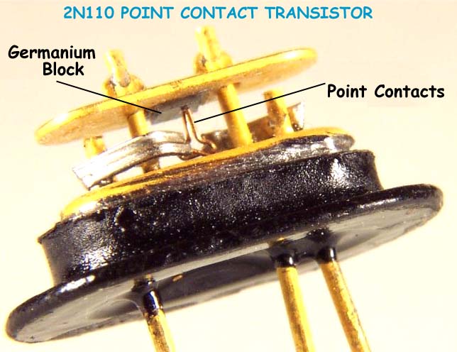
- Inside of 2N110 Point Contact Transistor w text, from Jack Ward - added Apr 22, 2015
|
Dear Friends, and others ;-))
Long ago, I (Ed Thelen) read a learned article (way over my head) in either the IRE or AIEE journal, (predecessors to the IEEE of today) proving that the new transistors would never be able to amplify above audio frequencies. Vacuum tubes would always be required for higher frequencies. Glowing cathodes are here to stay :-)) This has distorted my whole world view. :-(( - Well, sorta ;-)) |
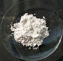
Powder inside an IBM 083 Transistor - from Robert Garner - July 5, 2022
|
While browsing my library yesterday, I opened IBM's LLoyd Hunter's 1962 Handbook of Semiconductor Electronics (2nd edition), for anything on desiccants.
On pg. 9-2 (in the chapter titled "Encapsulation", it says:
"PNP and NNP germanium transistors are very sensitive to changes in water-vapor pressure. Reverse current and current amplification will improve or deteriorate, depending upon the previous surface conditions. Very generally, however, it seems that NPN transistors are more sensitive to moisture when being encapsulated than PNP transistors.
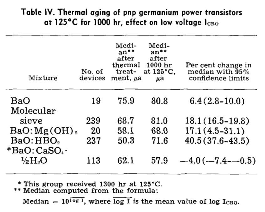
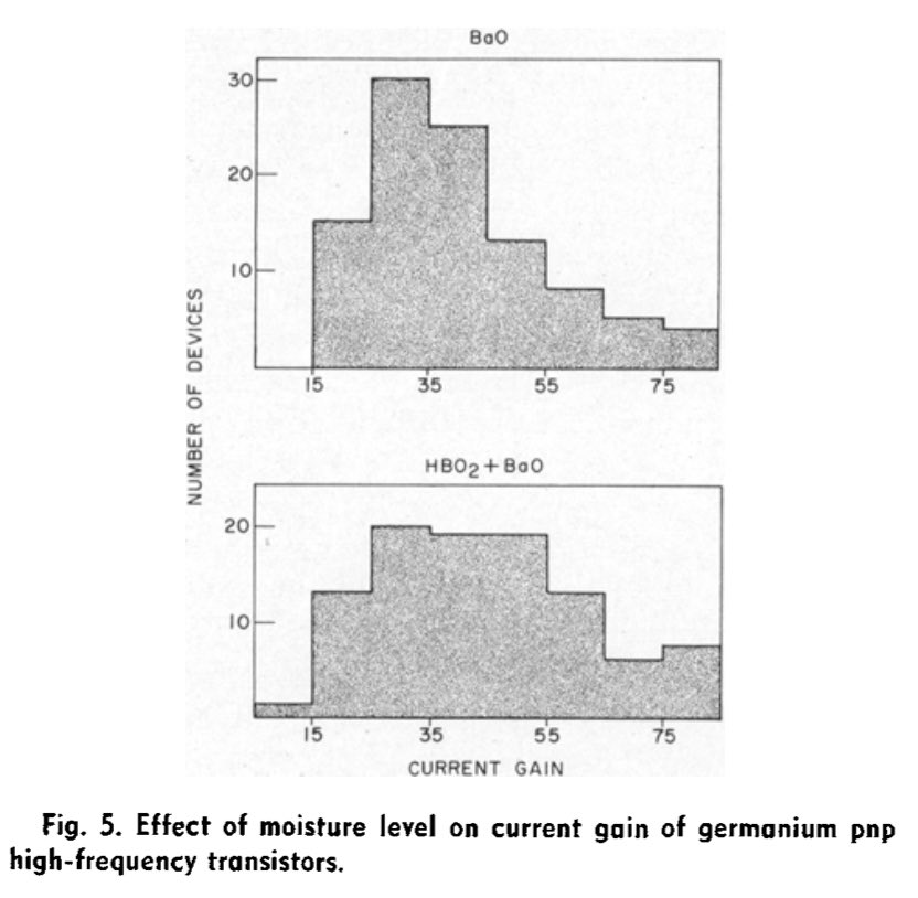
Googling, I found a 1962 article that tested the efficacy of barium oxide mixed with calcium sulfate and other desiccants in germanium transistors (calcium sulfate + barium oxide being the best). It also posits an explanation as to why water vapor messes with Ge transistor behavior.*
The powder I've seen in the IBM transistors indeed looks like calcium sulfate (gypsum); it's certainly not a "molecular sieve".
If our IBM transistors also contain barium oxide, look out - it's a skin irritant. And don't eat it:
Best Regards, - Robert
*
The article: "Selection of Germanium Transistor Parameters by Control of Moisture at Low Levels within the Device Encapsulation”, Robert J. Gnaedinger Jr., Steward S. Flaschen, Marie A. Hall and Edward J. Richez, Journal of The Electrochemical Society, Volume 109, Number 7
I went ahead and purchased it, ... excerpts below should be OK. Excerpts: "These experiments have indicated that moisture vapor in air within the sealed, device encapsulations has a pronounced effect on the surface re- combination velocity of germanium transistors at extremely low relative humidities, relative humidities as low as 10-8% (0.2 ppm)."
"It is well-known that the chemical composition of the gas phase adjacent to a semiconductor surface plays an important role in determining the electrical properties of that surface (1-3). Water vapor is perhaps the most striking example of this fact. High relative humidities produce severe and erratic current leakage paths across the surface of silicon and germanium crystals; changes in the humidity at moderate levels produce pronounced changes in the surface conductivity and surface recombination velocity. In the manufacture of semiconductor devices it was this high sensitivity to changes in the moisture level which caused the introduction of hermetic sealing of devices. Yet, although this hermetic sealing generally removed the erratic behaviors associated with gross moisture, there remained day-to-day, seasonal, and aging variations in the parameters of production devices. In order to reduce these variations, it was found necessary to insert moisture adsorbing materials into the hermetically sealed device encapsulations. This technique yielded a more reproducible product, but it frequently accomplished this at the expense of large shifts in the levels of some of the device parameters.
“The data presented above indicate that certain parameters of germanium transistors depend very sensitively and reproducibly on moisture partial pressures at levels from about 80 ppm to below 1 ppm in air. The parameters thus affected are those which are strongly influenced by surface recombination velocity (or surface generation rate). The simplest interpretation to be made of these observations is that even at these very low partial pressures, sufficient water is adsorbed onto the germanium (or germanium oxide) surface to affect the surface properties appreciably. According to the work of Law (14), monolayer adsorption of water onto a germanium surface does not become complete until a relative humidity of about 10% is reached (this relative humidity in air at 1 atm pressure at 25~ corresponds to about 2000 ppm of H2O). Consequently, the present results suggest that water plays perhaps its dominant role in affecting surface recombination velocity in the region below one monolayer, a conclusion that is consistent with the work of Law and Meigs (4).
|
Mystery Solved: Very, very early experimental point contact [transistors], from David Laws November 16, 2015
FYI
David Laws ________________________________ From: George Keremedjiev [ director@compustory.com ] Sent: Sunday, November 15, 2015 5:26 AM To: ... Subject: Mystery Solved: Very, very early experimental point contact transistors Gentlemen: An update... I believe that these two transistors are among the earliest of the first experimental point contact transistors in existence. Thank you for your help. Best, George George Keremedjiev Director American Computer Museum Bozeman, MT |
From: Rick Dill < rdill@cyburban.com > 09/03/2008 10:12 AM To Robert B Garner/Almaden/IBM@IBMUS cc: ... Subject Alloy Transistors Robert, The early 1950's were an interesting time. In the summer of 1951, Bell Labs had a "summer school" for a fair sized group of university professors. The professor who taught optics attended and had lectures from the likes of Shockley and Bardeen as well as some laboratory hands on time. They published a paper with everyone as an author in which they confirmed the Einstein Relationship between drift of electrons and holes under electric field and thermal diffusion. They returned to campus with a small kit of experiments which a fellow student, Jim Boyden and I latched onto and used both for recreation and every opportunity for a project. We were sophomores when we got our hands on this. It included a germanium alloy diode for measuring IV curves, a chip of germanium with rhodium plating on the back (which we had to learn how to replace after etching it off) to be used for making point contact transistors, and a bar of germanium for the Shockley Hall measurement of drift and diffusion of electrons. We fabricated our own point contacts and crude manipulators to put them down near where we wanted them. In the summer of 1954. fresh with a B.S. in physics I had a job at IBM in Poughkeepsie. It was my first industrial research experience and a wonderful experience. Joe Logue was the manager of the small group which included Hannon York, the engineer who invented the current switch circuit (non-saturating), Bob Henle who was a really good circuit guy and lead the company a few years later to abandon core memories and go to semiconductor memories. At the time, the group was just off of the CRT based electrostatic memories used in the 701 and the later mica target CRT-like memories used in the following computers up to the introduction of magnetic cores which were just coming visible in 1954. My assignment was really a gift. Joe wanted higher function circuits with the example being the neon ring counter. As he has told you, with no real hands on experience I was able to postulate that we might be able to produce such a thing with a double-based diode (unijunction transistor) which had multiple emitters and with the help of the small group in the pickle factory actually get a four-state device prototyped. Dick Rutz and John Marinace were the key people in that group and I eventually ended up working for in Rutz's group. I also postulated an adder circuit based upon the Shockley Hall structure, but with deflectors to steer the electron cloud sideways to multiple collectors. We didn't make this, but it did show up a decade later as an academic achievement. While Bell Labs was stuck on point contact transistors (and even made a computer out of them), Joe Logue has recognized the superiority of junction transistors. From a circuit standpoint, the ones available had too much base resistance to work well in digital circuits, although this didn't hamper them for communications. He tried to encourage the vendors to make transistors with low base resistance to little avail since computers were not important to the electronics world at that time. The task got handed to Research where on the fabrication side the team of Rutz and Marinace and their technicians made alloy transistors with a small alloy emitter surrounded by a circular base contact, and a larger collector junction on the back side of the die. Contrary to what most people believed, alloying was a well determined metallurgical process when done right. To do it right, you needed the crystal to have a <111> orientation. This is the slow dissolving direction when subject to dissolution by molten metal, so the sides of the dissolved region were angled along <111> planes and the bottom flat. The depth depended on the volume of the alloy "dot" and the temperature. On cooling, the germanium first cleanly regrew precipitated from the melt and was doped by the materials in the dot (indium gallium for PNP transistors and tin antimony for NPN). The collector on the backside was simply larger and etched more deeply into the germanium chip. The design was IBM's, but we went to TI and contracted with them to manufacture germanium transistors for us. We were allowed only to make 10% of what we needed, which gave us room for special applications such as core drivers or advanced devices before releasing them to TI. In spite of Joe Logue trying to get me to stay and do graduate work in the Syracuse MS program, I went back to Carnegie Tech and moved from physics to EE. 18 months after that Bob Henle visited campus following up on a summer job one of the young faculty had a year after me. IBM wrote three separate contracts. One supported my research with the requirement that I come to Poughkeepsie roughly monthly to report on my progress. The other two supported Dale Critchlow, the young faculty member, and Bob Dennard, one of his students. Both Dale and Bob were working in magnetics at the time. I was the first to join IBM in February 1958 and Critchlow and Dennard joined the following summer. We were all in the same group trying to do circuits with multi-hole magnetics and transistors. I left that project in summer of 1958 to go to Poughkeepsie and work for Dick Rutz with my initial assignment being to duplicate Esaki's work in Japan on tunnel diodes. In 1955, I worked at RCA Labs for the summer on silicon diodes and the observation that they did not behave according to Shockley's theory. There I met Herb Kroemer who is credited (among other things) as the father of the "drift transistor". Kroemer postulated (as a theorist) that a graded impurity doping in the base region would provide a field that greatly speed up transistors. It was only after I got to IBM that I read a patent of Lloyd Hunter which is the patent on the structure, so IBM has at least as much claim as RCA. By diffusing (probably phosphorus) into the germanium blanks, the IBM design became much faster. In 1958 on returning to IBM, I found that the development group had built a fully automated factory for producing alloy transistors. It used syntron sonic driven bowls to feed to germanium die, alloy spheres for emitter and collector, stub leads soldered to the spheres during alloying, and the dished base contact washer. These were fed into high purity carbon fixtures, one for each transistor. Once the assembly was together it went through a hydrogen furnace, after which the transistor was extracted, etched, washed, dried, tested, and then assembled onto a header. The carbon fixture was sent back to be re-used. This room-sized automated factory could product 40 million transistors a year, which was more than IBM needed. We shipped the factory to TI with the stipulation that they could use it only for IBM production for a stated number of years. When the diffused base transistor came in, it was only a small modification to the line to get the die right-side-up so that the diffused surface was facing the emitter. About 1964 I visited TI and saw multiples of this production facility running full tilt to make germanium transistors for the world. Silicon really came in with the system 360. The group that met to work out what would be done was the Compact Committee. I was a research rep on that team. We should talk about that sometime. Bill Harding was one of the key people and I believe that he is still around in Southern CA. What became solid logic technology (SLT) came from his declaration that he could produce individual transistors very cheaply and solder them directly to substrates. This was all an act of faith, but it came to fruition and significantly delayed IBM's serious entry into integrated circuits for logic. When we did get into integrated circuits for logic, electron beam lithography played an immense role in giving IBM a competitive advantage. Hans Pfeiffer was the leader in this technology and is now in Carmel Valley. This is just a little background for ou[r] Thursday discussion. Rick |
After the meeting with Rick, Robert Garner wrote
I met with Rick for 3 hours today.
He was a PhD summer intern at IBM in 1954,
    working on multi-emitter Germanium devices.
Fascinating conversation on all what was going on a IBM at the time (and later).
He thinks he can  explain our loopy I-V curves
    (water contamination causing the usual culprit - surface states.)


Finally I have someone to talk to about the physics and manufacturing
    of our alloy junction transistors. (although I have some old books on topic now too.)
He also talked about how hard it was to make the
    high-voltage core/hammer driver power Ge transistors...


- Robert
|
>> Have you seen early Philco transistors -- "look a bit like bullets >> - about 1/2 inch long, and maybe 3/16 inch diameter, >> metal with a rounded top" -- on any SMS cards? 
> A Google image search of 2N501 will show somw Philcos. > >> (I can send higher-res versions of these pics if you need.) > Yes, please. On early transistors, sometimes the distinguishing marks > for each manufacturer are very subtle. > > Thanks! > > -- > Will |
From: Rick Dill
Sorry for the late response, but I've been off-line for a couple of days
in the Sierra.
Philco had some of the most interesting transistors of the 50's era.
There were three families as the technology developed.
All their transistors were made by a very interesting process. They
started with the germanium die connected the the base contact ring in an
manner essentially identical to the IBM germanium transistors you are
used to.
This is then placed between two glass capillaries which served as fluid
nozzles for very fine jets of fluid. The two nozzles differed in
diameter and diameter of stream with the one on the collector side being
larger.
These are used to get two jets of electrolyte impinging on the two
exposed sides of the die. The fluid is an electrolyte which contains
both indium and gallium in solution. A voltage is applied between the
base ring (die) and electrodes in each nozzle. Initially, the polarity
used causes electrolytic etching of the germanium, creating relatively
smooth flat bottomed indentations from the two sides of the die, with
the collector being deeper and wider.
This etching process is monitored by an infrared beam which goes through
the fluid and nozzles. When the infrared transmission rises enough,
the etch process is stopped and the current reversed. This plates a
thin metallic film of indium/gallium (mostly indium) circular film.
Leads are attached to these films for the emitter and collector
contacts. The resultant transistor is packaged in the "tiny bullets"
observed. The base region could be etched down to where it was very
thin with an accurately controlled thickness.
The first of these was the "surface barrier" transistor. It used the
metal-semiconductor barrier (schottky barrier) for the emitter and
collector. This worked OK for the collector, but the emitter wasn't
very efficient and the transistors had low current gain compared to
competitors. Where they won was on high frequency response.
The next step was to run the finished transistors through a very brief
thermal cycle and to slightly "alloy" the emitter and collector films
into the germanium. This produced consistent high frequency transistors
that were superior to anything on the market. The drawback was that
they were fragile because of the very thin membrane base. In the summer
of 1954, when I was a summer employee, the circuit team under Joe Logue
was investigating these (Jim Walsh, Bob Henle, Jim Mackay, and Hannon
Yourke). They ended up rejecting the Philco SBT and Micro-Alloy
transistors because of ruggedness concerns.
In 1955, I was at RCA Labs for the summer. My assignment was to look at
the forward I/V curves of silicon diodes (which I made). They did not
follow Shockley's theory! That was explained a few years later in a
classic paper by Shockley, Noyce, and Sah,
A new employee at RCA Labs was Herb Kroemer, just arrived from Germany
where he had published a paper on the "drift" or diffused base
transistor. Kroemer had correctly worked out the physics which showed
that a base region which had an impurity grading from highly doped on
the emitter side to low on the collector side would have an internal
electric field which would propel minority carriers from the emitter to
the collector. RCA immediately put these into manufacturing, as did
many including IBM which modified the automated transistor machine to
make them.
The actual patent for the graded base structure was actually held by
IBM. More on that later!
Philco was quickly able to adapt their process to work with a die which
had the base region diffused from one side. They adapted their etching
so that the emitter etch depth was very small, while the collector
etched deeply into the die. Again, their IR control allowed them
precision control of the physical width of the base membrane. This was
called the "micro-alloy diffused transistor". Exceedingly good
performance for the day, but they continued to be mechanically fragile.
I probably have some philco transistors in my collection. One of these
days, I will unearth that and see what is of interest to the computer
history museum.
Rick Dill
The prototypes for the 1401 were undoubtedly made by two technicians who worked for Dick Rutz. Rutz did most of the exploratory device fabrication. The technicians were Ralph McGibbon and Earle Harden. They were masters of the build-by-hand exploratory germanium transistors.
Rutz pretty well demonstrated that the "forming" of the collector on a point contact produced an np junction at the collector which was why point could have an alpha greater than one. He also made a two collector point contact transistor which could perform the full adder function. That was in the summer of 1954. He also got some prototypes together for me to demonstrate the concept for a decimal counter based upon a multi-emitter unijunction transistor. That was my first integrated circuit.
In 1959 I joined Rutz's group where I learned to build transistors by hand, but without the amazing steady skill or McGibbon and Harden. My project was to reproduce the Esaki Diode (later tunnel) simply by reading Esaki's publication. Before long Earle Harden worked for me and we got into 3-5 tunnel diodes, high efficiency GaAs LEDs and IBM's first injection lasers.
Earle, in addition to being an incredible technician was an amazing master mechanic. He was key to a mask camera I was making to get no placement errors in overlay. The David Mann steppers were open loop lead screws and .... I will come back to this in another post later about mask making for SLT and beyond. Earle also defined the head lapping process for the first thin film magnetic recording heads. That same process is still used by every manufacturer or disk drives today.
Yes, in development and manufacturing, many jobs went to women. That is still true today.
Threading magnetic cores was commonly done by women who handled the care and dealt with frustration better than men, although in the beginning when the process wasn't stable, it usually was done with men who were brought to a much better understanding of why and how things were done.
IBM built machines for automatic threading of core arrays. These got more complicated as cores shrunk to smaller sizes to get faster switching, lower currents, and more cores per unit area of the array. My understanding was that the automatic core wiring machines vs humans doing the wiring was pretty much a wash and that both process options were used.
On the 650, that was the machine I first used. A close friend, Karl Konnerth, introduced me to programming and the 650 by handing me something like a 20 page instruction manual for Wolontis emulator that ran on the 650. It took half the memory (1000 words) for itself and gave the user the other half. What the user got was a 3 address floating point image and yes, it did run slowly. Still I was trying to model unijunction transistors for my PhD thesis and I needed numerical help with the non-linear differential equations.
Carnegie Tech had just gotten their first computer, an IBM 650. It was for education use and not administration. Karl got into the machine from assembler on up. SOAP gave the assembler control of assigning memory locations so that when an operation completed, it was stored in a location coming up soon. Karl and I worked together over the years. I got him to come to IBM for a summer to see how quickly we could turn a semiconductor laser on or off. I felt that this device was likely good for optical communication and he concurred. The answer was simply "faster than we can measure"
Over the years Karl and I spent a lot of time working together. He was involved with a Fishkill engineer in an optical communication demo at Expo in 1966. He and I created measurement tools for semiconductor manufacturing in the 1970's that also resulted in IBM trying new product areas. One in technical areas where our thin film measurement tool was offered to the semiconductor industry and to the fabric industry for color matching and dye usage. This was IBM instruments, which didn't survive. Our Fishkill partners wanted to be like HP or other standard measurement tool things. Our tools were also way ahead of their time. The other area a few years later was the formation of an IBM product group in medicine with the key product a hospital cart sized unit that acquired ECG data and performed an amazing level of analysis of even very difficult traces. That also failed because once you have a trace, the physician attending can tell if it is "normal". If not normal it goes to a cardiologist. At the very highest level, it treads on the egos of the very top guys who wanted to be paid for the answer rather than be told it. Karl came with me to Fishkill when we were setting up the last two bipolar factories. He took a small team and created the first fully paperless semiconductor manufacturing line ever. Now in his mid 80's he is still playing with single board systems. He might be a person of interest for CHM.
enough for tonight. This will go out without proof reading. HELP.
Rick
David Laws - Jack Ward, Early IBM Transistors - Feb 15, 2015
Jack Ward,
principal of the online
Transistor Museum,
has generously donated many important historic transistors to the CHM collection. He is currently working on a new collection that
will include early IBM devices, including types used in the 1401.
Attached you will find a draft copy of the text that will accompany the donation. Please forward the document to any and all members of the
1401 team who may be interested, If you have any comments or corrections
that you wish to send to Jack please contact him at the address above.
David Laws
TransistorMuseumIBM-GermaniumComputerTransistorHistoryDraftFeb2015-2.pdf
Comments by Robert Garner - Feb 16, 2015
This article reports an assembly rate of one transistor every two seconds, but later sources say one per second.
There's one photo of one station of the (remarkable) assembly line.
I wish there were some photos of the entire line (likely in TI's archives.)
- Robert
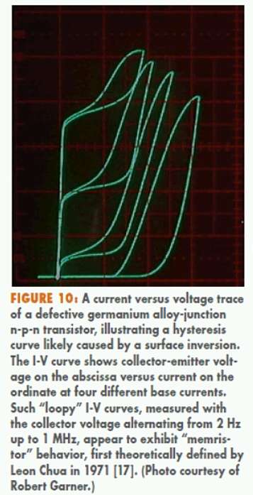
The reason I've been exploring the history of the physics and production of germanium transistors is to gather clues as to why some exhibit memristor-like loopy I-V curves. There are some references to loopy germanium I-V curves, including the very earliest characterization papers on germanium. Do you know any semi-conductor device physicists who could help?
I included this photo of one of our loopy I-V curves in the ISSC 1401 article (strange place for a computer history article), hoping that it might pique someone's interest enough to contact me. No nibbles.
IBM Almaden Research, San Jose, CA
From: Robert Garner
Jack,
Thanks for your follow-up, especially on your 077 PNPN germanium thyratron transistor.
It would be interesting to characterize.
And I wasn't aware of Hunter's patent.*
I haven't taken a part one of the tall case types, but would be willing to donate
one of these if you have any interest in case dis-assembly and photos,
as you did with the TO-5 case.
Yes, it would be a pleasure to open one up (if there's a "surplus").
Thanks very much for the 1960 Electronics magazine article on the IBM automated assembly system.
I have looked for that for a while, and this is very helpful.
If you need a better quality scan, I could secure one at the San Jose (State Univ) library which has the period Electronics magazines in its reference stacks.
(I was able to scan its paper on the notched disk storage prototype developed at the NBS in the mid 1950s, studied by the IBM RAMAC developers in San Jose.)
Speaking of characterization, are you aware of (or have observed) the loopy I-V germanium transistor curves I mentioned/showed below?
Cheers,
- Robert
* I have a copy of both the 1st (1956) and 2nd edition (1962) of the Handbook of Semiconductor Electronics, edited by Hunter.
transistormuseum@aol.com wrote: at 5:32 PM
If you'll supply an address, I'll mail you some of the early 1950s/1960s IBM germanium transistors for your research, so you can characterize performance of a variety of these, as well disassemble a "tall-case" unit. Should be very interesting indeed.
I haven't done much in terms of electrical measurement and performance characteristics, although I do have some experience with point contact transistors and other negative resistance devices such as tunnel diodes, unijunction transistors and Shockley diodes. I can provide some of those 1950s devices as well if you are interested. Let me know.
Did you record or transcribe your interview with Joe Logue? I'd be very interested in reviewing this.
best regards,
Jack
PS - I'm traveling on business so it will be couple of weeks before I can mail the transistors.
PPS - I've attached another pdf,
this one decribing some historical germanium transistors used in the first U.S. satellites (Explorer I and Vanguard). Not sure if you are interested, but thought the description of germanium transistors in space would be useful.
Robert Garner to Jack transistormuseum@aol.com, at 8:16 PM
Thanks in advance for sending some of the earliest IBM germanium transistors (btw, I also have some) and the "tall case" unit to disassemble/photograph.
Yes, I video recorded my interview of Joe Logue. He was a strong outspoken leader.
Thanks for the article on the Vanguard transistors.
On this note, I've wondered why the 1401 didn't use the faster diffused base transistor.
btw, I have a fairly thick reference book/catalog of all the extant transistor manufacturing firms in the late 1950s (w/ transistor types, specs, etc).
Cheers,
- Robert
from Rick Dill to Robert Garner, Feb 25, 2015
I was there at IBM when this all was happening. As a summer student working for Joe Logue in 1954, I saw a lot of his operation, which was much more a circuit based engineering effort looking for what would really work for computer circuits. There I saw the Philco transistors with very thin controlled basewidths first in surface barrier electrodes, then the same with micro-alloy (much better emitters and collectors) and a few years with micro-alloy and diffused base. Logue had two key engineers, Bob Henle and Jim Walsh. All three became early IBM Fellows. The Philco transistors were perhaps a good model with a ring base, but they were mechanically very weak and a little vibration would fracture them. At the time they were the best for switching speed.
The research group in 1954 included a few basic physicists brought to Poughkeepsie from Watson Lab on Columbia campus and a very small and practical group of engineers and chemists including engineer Dick Rutz and chemist John Marinace. In my assignment from Logue to make a functional electronic device like a counter, I got to know both of them in trying to prototype my unijunction counter device that summer and later worked closely with them. It was Rutz who built the prototype devices for what went into the 1401 and beyond. Both Rutz and Marinace were very productive inventors with Rutz concentrating on devices and Marinace on process.
Using point contact-like transistor technology (pnpn .. hook collectors), Rutz invented a point conact-like full adder transistor, which I believe that I have given to the CHM. In 1954, there wasn't really any development activity.
In spite of Logue's trying to convince me to not go to grad school, but stay with him and the Syracuse MS program, I went back to CMU and set up the first lab there that could make transistors with a capital investment of only $1000. That served to build unijunction devices that I used to write the first semiconductor device related thesis in the EE Dept. I was basically without an advisor, but was greatly helped when Henle came to CMU and brought 3 research contracts for myself, Dennard (DRAM) who was then working on magnetics, and Dale Critchlow who had a great career at IBM culminating with deep trench dram chips. My contract required me to go to Poughkeepsie monthly to report on my progress which got me some guidance and lots of access to 650 computers, often sitting with their covers off. My work, while not prominently published was one of the first uses of carrier flow in a semiconductor device. Yes, solving Poisson's equation, numerically. Yes it was 1-D, but it was the first real model for the unijunction transistor.
I came back to IBM after the 3.5 years it took to get my PhD. For about six months I worked on circuits using transistors and multi-aperture cores for logic to get a change and then went back to devices working for Dick Rutz in1958 where I was assigned to build tunnel diodes following up on Esaki's paper. That was great fun starting with germanium and soon moving along with the field to 3/5 compounds like GaAs or GaSb which had direct band-gaps and much higher on to off ratios (and remarkably short life for GaAs which came back a few years later with lasers).
Over those few years, IBM's research had moved to the 701 building which had just opened the summer of 1954 in the heat of summer without air conditioning. The 702 and 703 buildings had been erected and staffed with development engineers and scientists and a number of people from other companies with experience in early semiconductor manufacturing. I got to know many of these well because they were only a building away and, like myself, interested in making things more than basic physics which was the general tenor in the research lab.
In the 703 building (if I remember the number right) were a whole bunch of key people. Bob Slade has been discussed. Mel Klein did a rather amazing job designing a germanium transistor capable of driving core memories. This had to be capable of one amp pulses with a hundred volt against the non-linear inductive swing of the cores. Those were a key component in IBM's early core memory, perhaps more decisive than the cores themselves. Paul Low, later VP of the components division was there and went off to Stanford for a PhD and back. Ed Davis, an underrgrad friend from college came after his PhD at Stanford. He engineered the SLT module technology including the technology for making precision resistors our of screenprinted palladium oxide resistors trimmed to precision resistance with a narrow beam sandblasting. He was also CD president, a little before Paul Low. There was Bill Harding, but I'll come to him later.
Rutz did a good job with the transistor prototyping, more from just building things and paying attention than from design. The 1401 transistor was basically out of his lab. While Herb Kroemer who ended up at RCA is credited with the diffused base (drift) transistor, he is the physicist who first showed it mathematically. The patent for the structure was actually held by Lloyd Hunter who was Logue's boss in the summer of 54 and eventually moved to Stanford and University of Rochester. Years later Hunter taught me and my new bride how to fly gliders.
I was a research rep on the "Compact Committee", a broad range of people looking at the technology for next generation computers. We had system designers logic designers, semiconductor development people, and only a couple of us from research. This went on endlessly with little progress until Bill Harding stood up and declared that he could make a transistor for a nickel in silicon. That turned the whole discussion and became IBM's SLT technology that evolved though discrete transistors to small integrated circuits to modular design of circuits from building blocks. Bipolar was the thrust for performance reasons .. either small fast systems for small computers or full ECL for top end speed like the model 90. Both saturating and ECL were available to the designer.
I wrestled with Bill Harding some years later on process and manufacturing automation. Bill was very senior to me and what came out was an automated factory concept that got implemented in Fishkill for quick turnaround of IC's using electron beam writing for wiring logic chips to get unique chips out quickly. It also ended up somewhat in Burlington for memory chips. My end was developing automated process metrology for in-line measurement. Today's thin film measurement systems, both sprectral and ellipsometric tools derive from what we invented then. It was in that period that I put together a team to understand model and characterize lithography, which was probably the biggest contribution of my career.
Answers to some questions.
After my work on tunnel diodes and some diversion about the von Neuman scheme for making transistors using majority logic of parametrons (L/C circuits with non-linear diode capacitors). I moved back to GaAs light emitting diodes which physicists generally were excited because of their high efficiency. I got tied up with Nathan et al building devices which the theoreticians thought might be induced to lase. They were right and we published the semiconductor laser the same day as the team at GE. No Bell Labs didn't invent the semiconductor laser even though they claimed so in their 100th anniversry of the telephone publicity. That was great fun because I figured out how to make laser mirrors by crystal cleaving so we quickly had hundreds for any experiment anyone wanted to do. GE was still hand polishing up to just before I published my fabrication technique.
Bored with that and with silicon well established in the development lab, I went back to germanium one more time to see if, as a semiconductor with high mobility for both electrons and holes, we could beat silicon in speed. That was great fun because we ran a silicon project under Dave Dewitt and a germanium under my control, helping each other. Germanium won the switching speed race in 1967, but the physics of germanium suggested a much smaller advantage than my back of the pad start and we exited germanium (to our good credit).
From: From: transistormuseum@aol.com - Date: Thu, Feb 26, 2015 4:34 pm
On Thu, Feb 26, 2015 at 7:05 PM, < transistormuseum@aol.com > wrote:
I very much enjoyed your detailed discussion about early IBM transistor development. I have read Bashe et al IBM's Early Computers, which also contains much information about the early IBM transistor work, and your email discussion really adds much to this. I have a couple of questions which I'd like to pose:
Regards,
From: Rick Dill < rickdill@gmail.com > - Date: Thu, Feb 26, 2015 9:18 pm
Life is too busy now for me to go search for any artifacts I have, but I appreciate your collecting.
Now to answer your questions on point contact vs pnpn. I haven't read any books,but am looking back in my foggy mind. Hand made point contact transistors are a good point to start. What got me into the field was a summer course Bell Labs had for university faculty in the summer of 1951. The professor who taught optics, Leito, but was better known for his ability as an estimator for costs of brick work, went. Among other things was a joint paper by all of the attendees confirming the correctness of a long ago relationship between drift and diffusion of charged particles by Einstein. The important thing to me and to Jim Boyden, my friend, was the kit he brought home with experiments to use in teaching. Jim and I latched onto it and did one experiment after another whenever we needed a project.
One project was a germanium chip with a rhodium plated back onto which we were supposed to construct "microprobes" to place two point contacts onto the top surface. We found phosphor bronze wire and crudely pointed (I think with angled cutters) and I built some really crude things to get them close together on the surface. [In the process we etched the plating off the back and had to figure out how to replace it] So we made point contact transistor(s) and "formed" the collector with a capacitive discharge and they worked. That would have been about 1952. There were other experiments, like the I/V measurements of a grown p/n junction and a bar of germanium on which we could contact the two ends and inject carriers with one point and detect them with another to show the drift velocity and diffusion. It was part of the independent education of individuals! Jim was last in my view as the technical guy with Paul Allenon the X-Prize. He stayed in physics and I strayed into engineering and devices.
When I got to IBM in 1954 and then back a few years later, there were various views on the point contact. I never heard of the the work of Dickerson, but wouldn't be surprised. IBM was very deeply into germanium, even in the vacuum tube era. While some built computers using vacuum tubes for the logic, IBM early focused on using diodes for logic and vacuum tubes for amplification to the next stage. That meant that the speed depended more on the recovery time of the diodes, which got excess carriers stored if they were on very long, much like saturated transistor circuits. IBM worked on fast recovery diodes with Hughes, who made them for microwave receivers for the military mostly. To get fast recovery, the crystals of germanium were heated up to near melting and mechanically twisted to introduce mechanical defects. While the on/off ratio was reduced, so was the recovery time. These diodes were probably in the IBM 650 series that enabled my phd thesis. They would have been a good source of germanium surfaces which one could put point contacts on, particularly if one were more mechanically sophisticated than we were as undergrads.
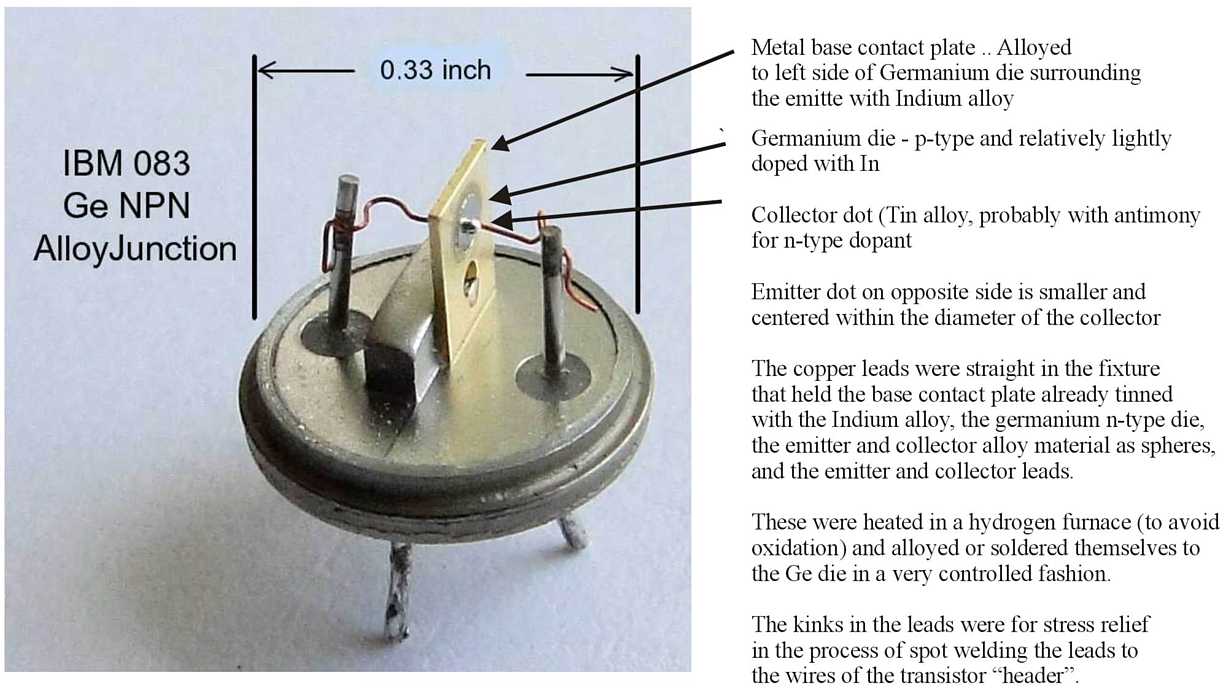
When I got to IBM the lore was that the current gain of the point contacts was really that the collector was a np junction from the phosphor in the phosphor bronze contact and the forming process. I can relate to that when we built diffused-alloy transistors later in germanium with an an arsenic doped aluminum alloy emitter into a diffused-base type substrate. With the right crystallographic orientation the alloy penetrated as a v-shaped trench and the arsenic diffused forward in the brief time at about 700C to form the base. The surface diffusion provided the connection to the base contact. With that we achieved raw switching times of 100 picoseconds, but that was in the 1960's with cooperation with TI who was making similar devices for low noise communication apps.
Joe Logue's team simply rejected point contact. The group had been formed after Joe had led the work on the memories for the 701 using surplus radar scope tubes. They had a hard engineering approach. Bell Labs did build a computer with point contacts, but it hardly made a peep in the growing technology.
Dick Rutz' full adder transistor was essentially point contact (i.e. deliberate np collector), and I don't remember exactly how he produced the collector. There were cigar box sized demo units which would add and display .. at very primitive levels.
..................................
IBM went to everyone in the industry to get someone who would build low base resistance transistors. That was a characteristic that Logue's circuit guys demanded. No one was interested. The washer shaped base contact was specifically for that purpose. TI, which was just moving up from instrumentation for oil drilling into semiconductors was the only one who stepped up. Everyone else thought that transistors were for communication and that base resistance didn't matter. At that point the group under Rutz had prototyped the transistors, as they did for several generations until IBM made the big change to silicon and SLT. I'm sure that the intitial orders were more modest, but I think that IBM was only allowed to build 4 million transistors a year. 1960 was early in the delivery cycle and the big production had hardly started. IBM also got power devices from Motorola and Delco as well as building some special devices like core memory drivers which needed higher voltage capability than was generally expected from germanium. There were also experiments with transistors made with deposited oxide on germanium .. something we came back to in the mid-1960's as we pushed for speed.
We did lots of things. I tried GaAs transistors after my experience with that material for tunnel diodes. I found it really hard to work with given the primitive technology I had. Still I was ready when the GaAs LED rush came in with the laser following.
Dick Rutz had assembled a small group of key technicians. Ralph McGibbon was ex-navy and steady building devices. Earle Harden was a master toolmaker, put together many of the leading transistors with his fingers, and was a master of precision machining. When I showed up with a new PhD, there was no office available, but a bench in the lab. They taught me as much of the trade as I was capable of learning. How to brace your hands so you could move the tweezers precisely. How to cut a shard of a tiny sphere of indium/gallium and heat it into a smaller sphere on a graphite hot stage for alloying. I learned the hard way to drink less coffee. The day they discovered that I wasn't just another technician was when the site tour guide brought the King of Denmark .. or something like that behind my stool as I was alloying on a hot stage and then introduced me as Dr..... I could see them in the background almost falling off their stools.
Earl Harden went on later ... still a mechanical tech .. to define the lapping process still used in making thin film recording heads, but that is a far different story.
and more dialogs - Mar 15, 2015
Let's look at the state of the art when the 1401 transistors were conceived. There were no silicon alloy transistors worth talking about. The diffused base transistors were brand new in the early 1950's and most of the first of them were implemented in germanium by RCA, following Kroemer's drift transistor theory. Interestingly, I believe that the patent to the diffused base transistor (the structure, not the theory) was held by Lloyd Hunter, who was Logue's boss.
The only silicon transistors were grown junction, which made narrow base transistors, but not in any volume manufacturing manner.
The IBM transistors were sealed in hermetic cans and had their surfaces etched and cleaned so that they were stable in a dry environment. The transistors you see are typical of transistors in open air since they have long lost their hermetic seal.
While the process for making them (either by hand or by IBM's automation) was fairly straightforward and if the thickness of the germanium was controlled, the sizes of the emitter and collector shot spheres correct, and the temperature cycle of alloying to spec, the yield of good transistors was reasonably high. In the automated manufacturing, they were tested and etched before being mounted on a header. The alloy process has messy edge margins that need general clean-up. With the right etch, the yield was high and the surface stable until mounted on the header and sealed in. There may have been a burn-in to eliminate flaky devices, but I don't recall whether there was. This certainly was required for early silicon transistors and ICs.
Semiconductor surfaces are not particularly stable, whether they have an oxide coat or not. Early work on silicon (until well into the MOS era) had most oxides contaminated with sodium which was charged and changed device characteristics and leakage, just with the application of voltages across the device. By the time we really understood how to make really stable silicon devices, the germanium era was past. It didn't have an oxide, but it was perfectly possible to treat the surface and then encapsulate the device to last for many years.
When the iron is oxidized or corroded out of the invar leads on germanium devices, they were no longer encapsulated. The GOOD NEWS is that enough devices still are reasonably encapsulated so that the 1401s work.
Even poorly encapsulated devices worked pretty well. The Raytheon hobby transistors were in plastic, but it was permeable to water and other contaminants. That didn't keep people from using them.
The big thing is that we did not the MOS technology, particularly MOS capacitors, to characterize surfaces. That really didn't become commonly available until the 1970's when I had some great fun with a summer student playing with it to look at both surfaces and point defects in silicon surfaces. I left germanium in the mid 1960's and easy surface metrology wasn't there. It was a decade until I had a lab with home built computer controlled measurement stuff. Since few had anything like we had at the time, lots of things were fun to look at, but there was too much going on to dig down and write papers.
Rick
"David Laws" < laws@computerhistory.org > 02/26/2009 05:03 PM
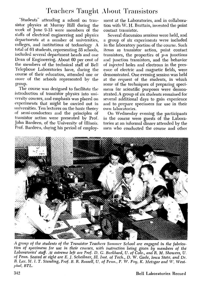
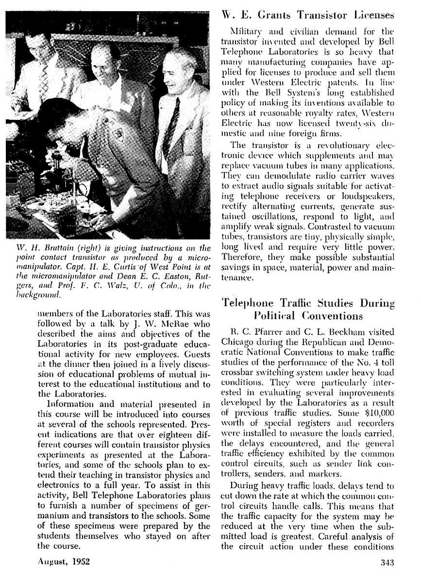
1952 Summer Course, kit - Apr 11, 2015
Your comments about the Bell Labs summer course for university professors back in
the early 1950s sparked my interest and I have been doing some digging through
the early transistor literature and think I came across some useful info on this course.
Attached is a two page scan from the August 1952 Bell Labs Record,
page scan 1,
page scan 2,
providing a couple of
photos and description of a course held at Bell Labs in June 1952. According to the article,
a total of 63 students (university professors) representing 33 schools attended.
Only a few names are mentioned, and I'm still looking for a complete list of attendees.
It would be terrific to find Dr. Leito mentioned. Notice there is a discussion about some
to the professors building experimental kits to bring back to their schools. Possibly
this is the origin of the kit that you and your friend Jim Boyden worked with.
I can find no specifics about the kit material that was developed for this course.
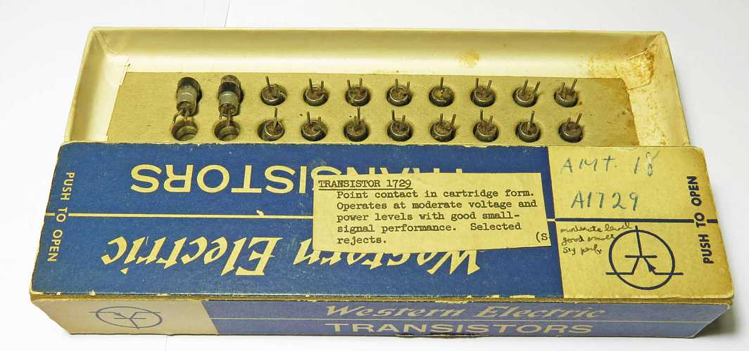
However, Western Electric continued this tradition throughout the 1950s and 1960s.
Attached is a photo of a 1953 set of cartridge type point contact transistors
which were performance rejects but were
packaged for use as study kits for universities.
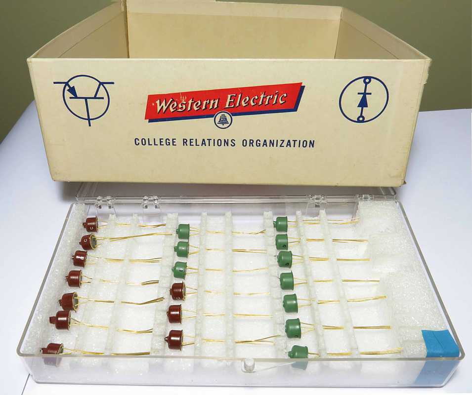
Also attached is a photo of an
early 1960s College Relations Transistor Kit.
One last note. The Bell Labs Record article also includes a discussion of the
transistor licenses that Western Electric had sold to twenty-six domestic and
nine foreign firms. I'm sure that IBM was one of the domestic licenses.
Thanks for your earlier comments that provided the inspiration for this followup.
best regards,
Jack
1952 Summer Course, Shockley-Hall experiment - Apr 12, 2015
I probably have the name of the optics professor wrong. There is one good way to access to a technical library (real or on-line).
The Shockley-Hall experiment (one of those in the kit) consisted of a bar of p-type germanium a couple of cm long. It had (I believe rhodium plated) contacts on the ends. The experimenters needed to connect electrically to these to get a known electric field and hole current. They were to place two point contacts on the bar and measure the distance between them (call the spacing between the point contacts 1.5 cm and the space between the end contacts 2 cm)
One point contact was the "emitter" which injected a pulse of electrons. The other was reverse biased and served as "collector" and showed increased current as the pulse of holes drifting down the bar passed it. The electrical pulse for the emitter triggered an oscilloscope and you could see how long it took for the electrons to arrive at the collector.
This was a great experiment. Jim Boyden and I set it up as one of the "projects" in a junior year experimental physics lab course. It was dazzling because you could actually measure the velocity of electrons under an electric field (electron mobility), which was usually done with the magnetic Hall Effect which was then being used to study carrier motion in metals and other conductors. In semiconductors, Hall effect measured the majority carriers, but not the minority ones.
Jim and I were asked to demo it for a department open house. After we'd graduated and he had gone on to Cal Tech and I departing for the local EE department, I was called back for Physics Open House evenings to set up the experiment and show it again.
This clearly was a one of the highlights of the summer course, The group of faculty observed that you could see the electron mobility, but you could also see the diffusion of electrons from the spreading of the pulse. You could play games and double the field applied to the bar and see the change in pulse shape. This resulted in a paper by everyone in on that demonstration and discovery.
The paper, published in late 1952 or 1953 (probably Physical Review) was the first verification of Einstein's theoretical relationship between drift and diffusion of electrons. If that could be found, I'd love to see it. It had a record number of authors since everyone in attendance at that demo was included.
Anyone have access to technical libraries. That is one thing that I think is wrong. Publication of technical papers is a large income generator for non-profits who get the material free, or even with payment (page charges). They then use the profit from selling journals at modest prices to individuals and extreme prices to libraries and companies. The reason for publication should be availability of the papers for advancement of the field by all. Having been in IBM, this was less obvious to me, but as I took part in IEEE at management levels (from society president to board of directors), it became clear that the model is wrong. Information should be FREE. It is in some fields, at least to many of the people who need it.
Any takers on looking for this article on Verifying Einstein's relation between drift and diffusion?
Rick
Date: Tue, Nov 30, 2010 7:38 pm
Hi all,
Some quick random inputs related to pieces of this thread.
from David Laws
Gentlemen,
I noticed that the transistor shown in the paper is slightly different from the ones that we use/photographed.
Our transistors have a much taller "tab base washer" that embeds the base disk within a circular cavity.
This design doesn't look as shock resistant.
![]()
p.s. I have over 50 scanned and photocopied articles (and several period conference proceedings) on the design and characterization of germanium transistors from the era. No one, including John Bardeen -- who closely investigated them for several years after his Nobel -- really understood fully how germanium transistors worked (i.e., unpredictable behavior and surface effects). Several papers corroborate how transistor production was a black art (i.e., how much atmosphere/humidity to allow into the enclosure, etc). There were conferences on germanium transistors to try to figure them out -- until, that is, silicon came along with it's more robust surface oxide layer. Tongue in cheek, I like to say we'd be living in "German Valley" instead of "Silicon Valley" if germanium had a robust oxide layer like silicon. ;-)
Manager, General Parallel File System (GPFS)
Office: 408-927-1739
Mobile: 408-679-0976
robgarn@us.ibm.com
To: Jack Ward transistormuseum
Subject: Re: IBM Germanium Transistor History and Historic Devices
Here an interesting movie of its tricks (taken by Bill Newman several years ago), with variable trace rates (including low frequencies):
http://www.youtube.com/watch?v=9lAvLXQEv2c
The 1st edition contains a "point-contact transistors" section that Joe Logue, in the oral history session (that I recorded at his home), told me that Hunter forced him to include. Joe had strongly felt that, with the development of the higher-yielding alloy-junction transistor, point-contact transistors were becoming obsolete, but some folks, including Hunter, especially given the initial high cost of transistor manufacture, were taken that "only one point-contact transistor was required in order to construct a trigger circuit." Rick Dill first mentioned this (impossible sounding proposition) to me and I didn't believe it until I read the section and saw its I-V curve with a negative slope (akin to a tunnel diode.)
Hello again Robert,
Jack,
I'll pass on the menagerie of negative resistance devices (for now anyway ;-)
I should create a DVD or upload it...
Looking at the page 4 transistor proto-family tree, it looks like I should properly say that the germanium transistors used in our 1401 are "3rd generation",
after the 1st point-contact and after the 2nd "early junction transistor"? (Up to now, I've said that the 1401 used the 2nd type of transistor ever developed.)
Were they that much more expensive, or perhaps more finicky?
Or why didn't IBM switch to a more reliable silicon transistor?
It's interesting that the transistors used in the 1401 were manufactured late enough to supply 1401s manufactured up until 1972 (and likely beyond for SMS subsystem(s), such as the 2821 used to attach 1403-N1 chain printers to S/360s.)
Most of the firms I'd never heard of.
If you don't have it, I'd be happy to loan it out or get a copy made . (I can supply its title tomorrow, as it's at work.)
Rick Dill, cc'd, also gave me a copy of IBM's course materials for their first transistor educational classes, and early Bell Labs instructional manuals.
Hi all,
Me, I was always restless and moving on. Still worked more across the lines to development than most in research.
and more dialogs Feb 26, 2015 - and a family tree :-))

... The attached "Semiconductor Ancestry Tree" might shed some light on this - this is found in a early 1960s WECO handbook "Solid State Devices".
Hi Rick,
Thanks in advance for your comments.
Jack [Ward]
Hi Jack,
Sun, Mar 15, 2015 9:32 pm
from Rick Dill
To: Robert B Garner / Almaden / IBM@IBMUS
cc: "Michael Riordan" < mriordan@ucsc.edu >, "Rosemary Remacle" < rremacle@computerhistory.org >
Subject
RE: Pics of early Kilby TI IC's made for IBM's Joe Logue in 1966 (and Ge Alloy-junction picture and loopy I-V curves and scan of 1955 "transistorized 604")
Robert,
Thanks for the interesting items of IBM semiconductor history. I'll talk to our oral history committee about the opportunity.
In the meantime I thought you might enjoy the comments of Morry Tanenbaum, the man who built the first silicon transistor at Bell Labs, regarding the vagaries of germanium devices. This is taken from an oral history panel on Silicon Research and Development at Bell Telephone Laboratories recorded late last year by Michael Riordan.
Tanenbaum: Germanium had some problems. First of all, its energy gap wasn't as large as one would have liked it to be, and so it couldn't operate very much above room temperature without cooling. The other problem was that it was highly surface sensitive. There was something called the ”friendly effect” that if you had a germanium transistor in an ordinary room, and waved your hand at it, and watched on the oscilloscope, the curves would wave back to you. So germanium transistors had to be carefully encapsulated, either in metal or ceramic or something, to control the atmosphere.
The photos of the two devices are examples of the discretionary wiring approach to building custom ICs developed by TI for the Air Force in the mid 1960s. We included a refence to this technique on the Silicon Engine at:
http://www.computerhistory.org/semiconductor/timeline/1967-ASICs.html
On Feb 28, 2015, at 9:02 PM, Rick Dill wrote:
Looking at the above:
The shut-down of the 360 transistor line just a month after announce was NOT made public. What I learned from it is translated to lessons not known by most of the silicon device world until people tried to make stable n-mos devices. There, IBM used the PSG as a top layer in its FETs and was able to make n-mos which was faster than p-mos because of the higher mobility of electrons. Dennard went around telling the world that N-MOS was the answer, even after people got to CMOS based upon his valid modeling and assumptions. Because of issues with latch-up and a poorly run CMOS program, IBM cancelled their project and didn't come back until everyone else whas there.
I don't recall the details of Mel Klein's transistor, but it was of the NPIN or PNIP type with a lightly doped layer between the base and collector to get the high breakdown voltage needed. That would probably have needed a lightly doped piece of germanium (I think it was too early for silicon at IBM). The base would have been diffused into that and the diffusion polished off the collector side. Then an alloy emitter and collector were used to complete the device. It was amazing to get germanium to do this heavy lifting at high voltage. Yes, it would have been too late for the 1401, but IBM was into core memories before Klein's transistor. I would need a very thorough refresh to understand the magnetic drivers used for the core memory, but I'm sure I could still get there.
Most of the circuit design came out of Joe Logue's team. Jim Walsh, Hannon Yourke, and Bob Henle were the key leaders. They and the others there may or may not have invented the circuits or derived them from other circuits of the day, but they would have been influential in the choice. The circuit voltages were large compared to the bandgap so use of complementary transistors made sense in getting from the output voltage down to something that could drive the same circuit. It had the complication that npn circuits could only talk to pnp and inversely, which was a design constraint. Some of the transistor transistor circuits had outputs that could feed the same type circuit, but looking for higher performance, it often was easiest to use the complimentary approach. This would be the case for the DTL and current switch circuits. While the TTL approach didn't require complementary transistors, diodes were cheaper than transistors in this era by a lot. As I said, diodes were the logic workhorses even in IBM's vacuum tube computers.
I loved applications of semiconductor capacitance, having made one of the very first voltage controlled oscillators. They allowed FM radios to stay on station even with manual tuning. I never was a fan of Von Neuman's scheme but management thought he was brilliant and we should work on it .. as did a Navy contract that loosely supported some of the work. I know more than you might ever want to know, even if it is incomplete. A computer using magnetic non-linear elements and fixed capacitors was built by Goto in Japan, but it was the only example ever built, so far as I know. Goto was interesting. I met him once years after his computer. He was on a quest fo find the magnetic monopole.
On reliability, you have a very biased view. The germanium transistors in the 7000 series, Stretch, and Harvest were very reliable and stable within the life of their computers. You are looking at 1401 transistors that are many years past any time that the machine would have been considered state-of-the-art. They were primitive early production and in their later years subject to awful environmental hazards. If you buy an Intel state-of-the-art processor today, it has a know lifetime. Now that is statistical, but the early failures are now screened pretty well. If you buy a flash drive for your laptop, you should be aware that it is designed to re-locate data as error detection shows up correctable errors and gradually it is loosing capacity. If you put it on the shelf, there is a good chance that in five years it won't operate. If you think you can put your pictures away on a hard drive and look at it a decade later, there is a good chance it won't work. That said, in the 1960's germanium project, our first challenge (in my mind at the time) was to achieve enough speed superiority over silicon that one might consider using an alternate technology. My back of the pad hoped for 4x at best. In the end 1.5 to 2x was the truth and no one would make the technology change. I was well aware that we had reliablity and other issues to contend with bit we were processing similarly to silicon and had an oxide film (not germanium) on the surface. I would never have claimed that we had either worked on or solved that problem, but it was solvable. The first GaAs tunnel diodes and lasers degraded in minutes of running. Today you take them for granted in your life for entertainment and communication. YES the reliability problem was harder than the problem of inventing or first building working devices.
When to get together to talk
Rick
On Sat, Feb 28, 2015 at 7:53 PM, Robert Garner
Rick,
Thanks for this amazing and informative history of transistor (and even laser) dev work at IBM. Sounds like you were able to work on the funnest stuff. We need to get an oral history session scheduled for you at the CHM. ;-)
>> Shortly after the announcement of the 360 a technician was etching the oxide before metallization and caused a shut-down of the line because of leaky transistors, which is how the role of the phosphorus was discovered at IBM.
As I recall from your first account, there's a little more to this serendipitous story. Can you please expand? ;-)
>> Mel Klein did a rather amazing job designing a germanium transistor capable of driving core memories. This had to be capable of one amp pulses with a hundred volt against the non-linear inductive swing of the cores. Those were a key component in IBM's early core memory, perhaps more decisive than the cores themselves.
Perhaps to late for the 1401, which doesn't directly drive the core planes, but uses a magnetic current amplifier core decode array.
>> It was Rutz who built the prototype devices for what went into the 1401 and beyond.
I still haven't discovered who invented IBM's CDTL (complementary diode transistor logic) circuit family used in the 7070 and 1401.
>> some diversion about the von Neuman scheme for making transistors using majority logic of parametrons (L/C circuits with non-linear diode capacitors)
If you can recall the details, I'd like to chat about this.
>> Bored with that and with silicon well established in the development lab, I went back to germanium one more time to see if, as a semiconductor with high mobility for both electrons and holes, we could beat silicon in speed.
Did you (or someone) figure out by then how to make a more reliable performant, non-flakey, repeatable Ge transistor?
> Do you have time to stop by the 1401 team again some Wednesday?
Cheers,
- Robert
Hi Rick,
On the 1952 Summer Course for university faculty at Bell Labs ...