Table of Contents
- Rick Dill's Comments on Ken Shirriff's
Germanium transistors: logic circuits in the IBM 1401 computer,
March 6, 2021
- TTL or CDTL or their origins generations before from Rick Dill, March 4, 2021
- from Joseph Logue about Max Paley, November 18, 2008
- from Joseph Logue - link between transistorized 604 card and SMS,
your card on display at CHM, August 30, 2009
- from Robert Garner, thanks for link between transistorized 604 card
and SMS, your card on display at CHM , 29 Aug 2009
- from Joseph Logue, link between transistorized 604 card
and SMS, Aug 29, 2009
- Re: Rick's Dills comments w/ more IBM stories on SSCS paper, 28 Aug 2009
- Robert's images of Rick Dill's donations in R|EVOLUTION
|
from Joseph Logue about Max Paley, November 18, 2008
From: Joseph Logue < jclogue@msn.com >
Subject: Max Paley
Date: November 18, 2008 1:39:52 PM PST
To: Robert Garner < robgarn@mac.com >
Hi Robert,
I am responding to your 11/16/08 e-mail on which I was copied.
I met Max Paley in 1953 after "Logue's College of Digital Knowledge"
had been completed and Ralph Palmer had agreed with my suggestion
to build three of the six machines that the class had "transistorized".
The group in the class that had studied the IBM 604 with the intent
of redesigning it around the transistor circuits and printed circuit cards
that my group had developed were transferred to Max Paley's organization
in the IBM plant.
In 1963 Bob Evans asked me to join the Systems Development
group reporting to Max Paley. I had responsibility for a number of programs
including all of the Stretch machines that had been delivered to England,
France, Los Alamos, etc. and project "Y". This was a very high performance
machine that would compete with CDC's high performance machines in the
future.
It became evident that there was a large mismatch between the effort
the IBM systems house was willing to spend on a future machine and
what the IBM Component Division was spending on a future technology.
I expressed this concern to Bob Evans and he a meeting with Vin Learson,
IBM's President.
At the meeting was Mr. Learson, whose name I have forgotten but who
replaced me as Staff Director of IBM's Corporate Technical Committee
when the government sued IBM in 1970, Bob Evans and myself. I told
Learson that IBM should decide when the next high performance machine
needs to be announced and then see that the Component Division and
the Systems Division do what is necessary to meet that schedule.
Learson turned to the guy that took over my job in 1970 and said: "What
do you think?" He said: "I thought we had it all agreed what we would do."
(This individual stuttered quite badly) After the meeting I told Evans that
I was very disappointed in the meeting.
On December 20, 1963 in a meeting with Evans, Paley, Phil Stoughton and
myself I told all three of them that they were headed for a lot of trouble
because CDC is going to sue IBM for having a paper tiger and I want no
part of that. (December 20 is my birthday)
In January of 1964 I had a new job in the Component Division and I was
in charge of the NGT Program where NGT stands for Next Generation of
Technology. I knew that integrated circuits were being developed in other
organizations and quickly found that that there was no work going on in
IBM except for FSD in Owego, NY. The Component Division assigned to
me a number of what I call "Cats and Dogs". These were programs that
the Component Division had accumulated but did not know what to do
with them. In fact the members of the Component Division were violently
against integrated circuits.
I learned much later, when I was Staff Director of the CTC, that in November
of 1963 the top management of the Component Division consisting of
John Gibson, Andy Eschenfelder, Erick Bloch and Bob Henle. Henle made
the presentation. In Henle's presentation he stated that integrated circuits
could never compete with Solid Logic Technology, SLT because with SLT
you can select only the good transistors to mount on the substrate whereas
with integrated circuits if one transistor is bad it fails the semiconductor
chip.
I lost track of Max Paley after he left IBM. Other than my disagreement
with Max's and Bob's blindly following IBM's upper managements improper
decisions we remained very good friends until their deaths.
Kindest regards,
Joe
|
from Joseph Logue - link between transistorized 604 card and SMS,
your card on display at CHM, August 30, 2009
|
Begin forwarded message:
From: Joseph Logue
Subject: RE: link between transistorized 604 card and SMS, your card on display at CHM
(was Re: Rick's Dills comments w/ more IBM stories on SSCS paper
(was Re: OK, here's the document.
Date: August 30, 2009 8:57:11 AM PDT
To: robgarn@mac.com
Cc: ...
Robert,
In my comment below I should have mentioned that the students were attending
the class to learn about transistor logic circuits. My small group of about five engineers
including myself designed the logic circuits and the printed circuit cards that the
students used when the three machines were actually built.
Joe
From: jclogue@msn.com
To: robgarn@mac.com
CC: ...
Subject: RE: link between transistorized 604 card and SMS, your card on
display at CHM (was Re: Rick's Dills comments w/ more IBM stories on SSCS paper
(was Re: OK, here's the document.
Date: Sun, 30 Aug 2009 11:47:02 -0400
Robert,
The students in "Logue's College of Digital Knowledge" were given three weeks
of class work on transistor logic circuit design and six weeks of laboratory activity
designing six IBM vacuum tube machines using the information they learned from
the three weeks of class work. For the 604 they did a cross section of the machine
not the complete machine.
The members of the class presented their work to Palmer in the graduation meeting.
After the graduation meeting I recommended to Palmer that three of the machines
studied be built. Palmer agreed and the transistorized 604, the transistorized small
accounting machine and the transistorized data communication machine were built.
The transistorized 604 was demonstrated in a number of cities around the U. S.
One criticism I received, from Lloyd Hunter, was that the transistor circuits in the
transistorized 604 were over designed because too few of the transistors failed
during the time it was demonstrated around the country. Which proves, you
cannot please every body.
Joe
|
from Robert Garner, thanks for link between transistorized 604 card
and SMS, your card on display at CHM
From: robgarn@mac.com
To: jclogue@msn.com
Subject: Re: link between transistorized 604 card and SMS, your card on display
at CHM (was Re: Rick's Dills comments w/ more IBM stories on SSCS paper
(was Re: OK, here's the document.
Date: Sat, 29 Aug 2009 23:50:31 -0700
Joe,
Great to hear from you!
Thanks for the missing link between the small, "experimental transistorized 604"
cards your class students designed and the real SMS card. I'll appropriately
update the SMS sentence in the paper, including your recommendation to use
wire wrap. Question: do you recall who actually came up with the exact card
dimensions, you or one of the students?
Did you get a chance to read the attached paper for the Winter SSCS magazine?
I would really appreciate your feedback on it. (I'll email an updated version
Sunday, with changes to the SMS paragraph.)
Your three key contributions: insistence on using alloy-junction transistors,
the pre-SMS card (with thick gold-coated contacts) and wire-wrap technology all
allowed the 1401 to be extremely reliable and to help achieve its status as
the most popular computer during much of the 1960s. Btw, we have NOT found
a single problem with a wire-wrap connection in either of the two 1401s
we've restored, nor a corrosion problem in an SMS edge connector/backplane connector.
Speaking of the SMS edge connectors: When we were trying to address the
question of whether we should apply a cleaning or anti-corrosive coating
(we elected NOT to!), I could not find any technical details on the metal
stackup on the SMS edge connectors, anywhere (patents, papers, etc).
So I asked the lab in Poughkeepsie to analyze the edge connectors.
Their report, based on "Energy Dispersive X-Ray Fluorescense" determined
the stackup to be 100 micro-inches (2.54 microns) of Gold
over 750 micro-inches of Nickel over Copper. No exposed Nickel nor
any signs of Gold porosity were observed. I don't think anyone has designed
PCB boards as robust as these SMS cards since then! (Gold thickness has
shrunk to almost nothing these days..) The report is here:
SMS_Tabs_IBM_Report_Dec2007.pdf
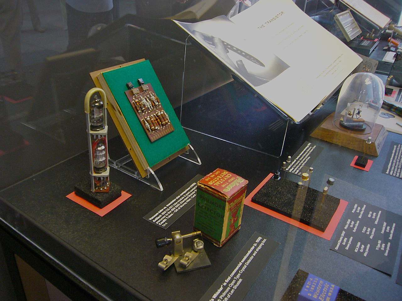
Btw, your transistorized 604 card is actually on display in the Museum's
new exhibit called "The Silicon Engine," pictured here:
(ironic name, given that most of the displayed transistors are actually Germanium! ;-)
And here's your card in the left back of the front case (mislabeled as
point-contact transistors still. Sorry!)
|
from Joseph Logue, link between transistorized 604 card
and SMS, Aug 29, 2009
|
Robert,
On page 5, in a Note it says: "I think Nate Edwards was the engineer
who actually defined the SMS format." This is not correct.
Please refer to IEEE Annals of the History of Computing,
Vol. 20, No. 3, 1998 the section entitled "The Movie". Ralph Palmer, my
boss had impressed on me that he wanted limited part numbers to
service future IBM semiconductor computers. I used the printed
circuit card concept that I had developed for the IBM transistorized
604 calculator. That card had eleven contacts, not counting
the six contacts in the two transistor connectors. If the reader looks
at Fig. 2 of the IEEE Annals paper he will see that the middle
contact connects to the same electrode of each transistor. The
conclusion is that if transistor connectors are eliminated from the
card and transistors are soldered to the card then the card will
require sixteen connectors for a single width card. This is what Ed
Garvey and I agreed to for the SMS card. Some executives did not
want to gold plate the card contacts whereas I insisted on gold
plated contacts and I was involved in the decision on the force
the contacts in the card connector had to provide for reliability.
After my involvement in many decisions of the type just described
I also convinced Garvey to embrace wire wrap because I had
become aware of wire wrap during a tour of Bell Labs. After I
produced the movie that dramatically showed how many part numbers
were needed to service the 700 series of computers and Bud Beaty
reviewed it and told Palmer if Tom sees that film Palmer will
get fired. I am sure that prompted Palmer to have Nate Edwards
replace me as the Secretary of Standardization if that was my
title at the time.
When Garvey headed up Manufacturing in the Components Division I was not
able to sell him on the technology of multilayer ceramic modules.
I was able to convince Karl Weiss of Boebiglen (sp) Laboratory and
he did a great deal of work leading to the control of the shrinkage
of the ceramic during firing. Because of the work of the NGT program
and Weiss' work Bob Evans was able to instruct the Components Division
to concentrate on multilayer ceramic modules, MCM, for the
Systems Division high end computers.
Joe Logue
|
Re: Rick's Dills comments w/ more IBM stories on SSCS paper, 28 Aug 2009
To: rdill@cyburban.com
CC: ...
Subject: Re: Rick's Dills comments w/ more IBM stories on SSCS paper
(was Re: OK, here's the document.
From: robgarn@us.ibm.com
Date: Fri, 28 Aug 2009 16:14:52 -0700
Rick,
Thanks for your interesting IBM stories and for reviewing the SSCS paper.
You didn't have any feedback on the changes I had made to your paragraphs,
so I assume they stand OK!?
Question --> Before IBM's automated facility to produce alloy-junction
transistors, had all alloy-junction transistors previously been hand made
(i.e.., no one else had any kind of automated facility ?)
For the benefit of the cc'ers, whom I know will be interested in your
interesting stories, I've extracted your long "Notes" from your review
of the paper, followed by any comments I might have. I prefix your comments
with my "text" as necessary.
Editor's note: Rick Dill's text (I think) is blue indented -
"By the 1950s, IBM had a huge installed base of users, operators,
and plugboard programmers and the rental of such “unit record” card
machines were very profitable..."
Note: This was some really amazing electro-mechanical equipment
on the industrial, rather than the desk-top calculator scale. The
electromechanical ability of Endicott was awesome. I have the hand-out
notes from the “new employee and summer student course” in 1955
I've been recording Fran Underwood's (1401 lead architect) history.
He was assigned to teach these classes in Endicott in this time frame, 1955.
Your class was in Poughkeepsie?
Can you please stop by sometime with your IBM class hand-outs
so I could make a copy!?
Perhaps we could meet for lunch at ARC, say Thursday the 3rd???
Note: Here [IBM 650] is where I got started. I was given a programming manual by a friend and a ten minute introduction to the computer, punch, card reader, and printer (probably the 402) by the same friend. It was a blast. There was little competition for time on it if you didn’t mind the middle of the night. You could play with auto-correlation for a statistics problem the whole class was working on. You could generate tables of trig functions (the life work of the head of the Math department). Oh, yes, you could try different approaches to numerical computation for solving Poisson’s equation in semiconductors and use it in your thesis.
Real programmers used SOAP (symbolic optimized assembly program) which selected memory locations to minimize the drum latency. I used a wonderful three-address, floating point simulator which used half the memory. It was Wolontis of BLIS (Bell Labs interpretive system)
Real programmers used SOAP (symbolic optimized assembly program) which selected memory locations to minimize the drum latency. I used a wonderful three-address, floating point simulator which used half the memory. It was Wolontis of BLIS (Bell Labs interpretive system).
Yes, at the time it was a “personal” computer and I soon was debugging my programs on the console which had bi-quinary read-out.
The 402 had considerable electro-mechanical arithmetic capability which one or two graduate students discovered and used instead of the computer. That quickly got stopped because the computer users couldn’t see their output without the printer.
Shortly after I left school, the CMU 650 got a core memory which greatly improved its performance. I never got to play with one of those.
Since at the end of grad school I was supported by a contract (from Joe Logue’s guys) and asked to regularly come to Poughkeepsie to report on my progress, I quickly learned how to find computers (often with covers off like the PC beside me) and get lots of extra compute time. You never left home without a card deck.
Have you read Don Knuth's "650 Appreciation" paper?
I'll send it in a speparate email...
Note: Yes, the vacuum tubes were unreliable. Most failures were loss of emission for one reason or another which eventually caused them to fall far enough from spec for the circuit to stop working. Actual burn-out happened, but was less common. Filament temperatures are relatively low compared to light bulbs. Gas in the tubes did happen and this gave a glow to the tube. I don’t recall many cathode to grid shorts in this era.
The Williams tube was simply a war surplus small radar CRT which had a tin oxide coating applied to the face surface. This was a single electrode used to detect changes in charge in the phosphor. The beam was positioned to a bit location (not raster scan) and then quickly turned on. There was an initial decrease of charge in the phosphor as more electrons were knocked out of the phosphor than came in. These landed nearby so the pulse was short, but detectable. If the bit had been written with a “1” there would be little or no pulse since the electrons hadn’t refilled that area of the phosphor. If the bit was a “0” it would be restored by deflecting the beam slightly to the side to restore the charge to the bit area. In the 1401 the cycle was 12 microseconds which allowed reading and writing or restoring one bit and refresh of something like 12 other bits. Joe Logue of course knows the details of this. I saw the hardware in his lab in 1954. I don’t know of a “dust” problem on the surface unless the whole tube face got conductive enough from dust that it became conductive and spoiled the sense signal.
One of our active 1401/unit-record volunteers, Bob Erickson, was the CE for the IBM 701 in Los Alamos. I've cc'd him on this email. He reported that he would "repair" flaky Williams tubes by dropping them face down on a hard surface, which reportedly disloged any accumulated particles from inner suface. He donated one of his 701 tubes to the Museum and still possess one. It would be interesting to try to write/read one again.
The IBM designed “Barrier Grid Storage Tube” was a home-built CRT with an internal target (faceplate) of a thin mica sheet. This had a grid in front of it to help control the flow of electrons ejected from the mica target. I don’t believe that they used a phosphor, but am not sure on that. This technology only held twice as many bits as the Williams tube and core memory was rapidly being recognized as a much better solution.
I may have a paper somewhere on this stoarge CRT...
Note: Bell Labs first really released the technology for the transistor sometime about the summer of 1951. That was when they held a large summer school for academic faculty. The professor from the CMU physics department who went came back with a small packet of parts and experiments. Another sophomore and I simply gave ourselves premier access to this and pulled one of the experiments up whenever we needed a project of a little entertainment for ourselves. He was Jim Boyden (most prominent recently as project manager for Paul Allen) in the quest for the X-prize. We made point contact transistors, measured the I-V characteristics of pn junctions carefully, and set up the Shockley-Hall experiment to measure speed of minority carriers in a bar of germanium. We used an old radar receiver scope to display the output. This also allowed one to verify Einstein’s relation between drift and diffusion many, many years after he had made the prediction. It also set me up well for a summer with Joe in 1954 and for pursuing my own course in life with this as a large element.
The announcement of the transistor was in 1948. Shockley’s prediction of junction and FET transistors were announced at the same time, but it wasn’t until the early 1950’s that work really started on the technologies needed to make and manufacture things that required extreme purity. Interestingly my father-in-law was involved in using chemical reduction of germane (GeH4) to obtain pure germanium for growing crystals.
One had to learn how to get and purify germanium (pure synthesis followed by zone refining), grow as defect free a crystal as possible, cut wafers aligned to crystal axes, etc. For point contact, the processing was fairly simple. One could take available wires and electrochemically point them and place them with micro-manipulators under a stereo microscope, pulse the collector wire to form it, and you had a transistor.
Alloy took a lot longer to become useful. Pure metal spheres of uniform size with precise composition were needed. These were done in shot towers, but manufacturability took people who know how to do precision shot tower operation for extremely small shot. For transistors of appropriate size for logic work, typical shot were from a tenth to a quarter of a mm with spheres for really high speed transistors eventually being 25 microns.
Polishing Ge was an issue. Mechanical damage from mechanical polishing left a couple of microns of damage below the surface. This had to be removed by etching, a technology that needed to be mastered. By the early 1960’s we were able to do a chemical mechanical polish which had no solids in the fluid and produced smooth flat wafer surfaces. In the 1950’s this was unknown.
Then there was the etching to clean up after the alloy process and leave the surface in an electrically satisfactory state and the need to encapsulate the transistors in hermetic packages, like tubes as you indicate.
It takes faith in progress and working with a whole lot of people to build the infrastructure. Joe had that.
BTW, at the time, the way BTL built junction transistors was by “growing the junction”. You started with one type of doping (relatively low for the collector) and started growing the crystal. You then put the counter dopant into the melt to provide the base. Then very shortly, you added more of the initial dopant to overcome the base dopant and produce the emitter.
You sliced a chunk out of the crystal more or less parallel to the growth front. They you cut a matrix of bars out, each one of which contained the transistor structure. With a contact made to each end, you could probe down the bar and discover where the base was and then alloy a contact to a base contact wire. While this was used for Ge to make thin base transistors, it was the only way known to make Si transistors in the early 1950’s.
It was the development of diffusion to create junctions in Ge and Si that both gave graded-base transistors with higher speed and also allowed silicon to become useful and eventually dominant for semiconductors. It wasn’t because the people working on Ge were dumb!
"In 1952, Joseph Logue joined IBM’s small transistor research circuit group after having worked on IBM 701’s finicky CRT storage tubes. He quickly decided that Germanium alloy-junction transistors were far superior to point-contact devices for complex digital logic circuits, ..."
Note: Joe is an engineer and a circuit guy. He was not ever part of the transistor fabrication or technology team, but he had major influence on the directions because he stood up as the “customer”. I was an engineer in the group under Dick Rutz in Research which did most of the technology. We were “practical” people in a sea of physicists interested in science. We built things, but were considered the bottom of the heap intellectually. We regularly turned the pile over and were on top for a little while. Lots of wonderful people and very bright people which made being there fun. I had great fun and my quest for intellectual breadth let me talk to anyone.
A couple of key people in the 703 building were peers of mine. Ed Davis was an undergraduate classmate and friend who joined IBM with the aim of becoming a VP. He eventually ran Components Division. Among his achievements was the resistor technology for SLT which gave the circuit designers precision resistors for high performance and good margins. He had an Apple II when the PC came out. He designed, built, and programmed a card for the PC which let him run his Apple software. I just checked. He is in Portola Valley. I will look him up.
The other was Paul Lo who was in the initial crew who took the IBM graduate fellowship offer up and got his PhD at Stanford. Both were in the 703 building in the early 1960’s and were part of my reason for straying from home in the 701. Paul ran Burlington for some years and then headed Components Division and was the person I talked to when I got mad at Watson in the late 1980’s and walked out of my management job into an assignment with the small team that put IBM’s last two bipolar factories in place. I believe that Paul is still living in Greenwich CT, but haven’t done a search.
All of us were pilots at one time or another, as was Joe. Both Ed and Paul had executive ambitions which they achieved. I never had that, preferring to be paid adequately for doing what I loved to do most .. staying right in the details of the technology and working directly with technical people.
I was one of the few who talked to the people up in the 703 building to see what ideas they had. I also talked to the magnetics people, system designers, software people, etc. I had a good friend that I met in the Army, Jerry Amos, who I got hired to IBM. He spent his career in product test keeping IBM honest when they announced any product (If it doesn’t meet the spec, either fix it or change the spec). He had an amazing time, probably working on testing the 1401 and ending up on the Z series. Never moved and never changed his job. He’s in the Boston area.
I didn't find Jerry Amos's name in our 1400 family people list (incl manufacturing and test).
"As IBM had earlier decided not to manufacture electronic components itself, in October 1959 they shipped their transistor manufacturing facility to Texas Instruments (TI) with the stipulation that it only supply transistors to IBM for three years. TI eventually replicated the room-sized facility, supplying Germanium alloy-junction transistors to the world."
Comment: TI was a company building custom instruments for the oil drilling market which had just decided to branch into the transistor radio business as a new venture supported initially with the profits from their original business. They licensed TI’s technology and built a staff of very competent engineers and scientists. It was there that I saw the process of producing grown junction transistors. They were very interested in expanding their transistor market when IBM approached them, in marked contrast to everyone else. The TI/IBM supply chain was a major element in building the company that they are today. IBM didn’t want to manufacture transistors unless they really had to in order to focus their efforts on designing their products. One has to remember that IBM wasn’t a very large corporation at that point.
Based on this new info, I updated the "TI" paragraph to:
"IBM’s transistor assembly facility could produce 3,600 transistors per hour, or hypothetically, 30 million transistors a year, far more than IBM needed. As IBM had earlier decided not to manufacture electronic components itself, they approached Texas Instruments (TI). TI, originally a provider of oil exploration instrumentation, had recently branched into the transistor radio business and were open to expanding their transistor market. In October 1959, IBM shipped their transistor manufacturing facility to TI with the stipulation that it only supply transistors to IBM for three years. TI later replicated the room-sized facility, supplying Germanium alloy-junction transistors to the world."
btw, here's a picture of one of a TI 21-track T-961 tape deck, something I had never heard of until I interacted with the folks at this Aussie data recovery company: http://www.spectrumdata.com.au/content.aspx?cid=189
"During this time, IBM was also looking to automate the production of solid state printed circuit boards. Edward Garvey, designer of the 700-series tube module, after witnessing a proliferation of over 2,000 module types, saw the need for an automated facility for producing many types of transistorized logic cards.."
Note: I think that Nate Edwards was the engineer who actually defined the SMS format. I don’t know that for sure. He was interesting and was part of the tag team of four who Ken Powell (IBM Education) used to teach any executive who would sit still individually about what a computer was. That course was extensively given and never on the books. All the team, except for Ken worked for me and I simply let them have the time they needed. This was one of the things that helped soften up management so that the PC could happen.
Would you have any idea whether Nate Edwards could be contacted/found!?
Note: A key element of wire wrap is that it can be easily repaired or changed in the field.
So noted.
"In 1961, a bank check optical magnetic character reader and 1405 RAMAC disk drive (20 million characters) were offered, ..."
IBM built both kinds, optical 1418 and magnetic 1419!
http://en.wikipedia.org/wiki/List_of_IBM_products
"One key technology used in the System/360 was a flexible control store that implemented the S/360 instruction set via microcode instructions..."
Note: The control store of the model 30 was a punched capacitor card of standard IBM card format. It was programmed by punching to remove capacitors. All the small 360 computers were pretty primitive processors with extensive, but varied ROM control stores. You had to get all the way up to the model 90 before the full instruction set was directly implemented.
An aside was the IBM 5100 personal computer. It ran full APL\360. The processor was a four bit PALM microprocessor. It had something like 192k bytes of control store. In the control store, it emulated a full 360 and on top of that had the APL code installed. It was a landmark machine, but the original prototype shown to management was actually emulating the much simpler 1130 and running the APL subset for the 1130, which was a good, but incomplete implementation. The original show machine was much faster.
When we started using an 1130 for control of measurements and instruments, one of the interfaces we had was APL\1130. We took an unused instruction area and made it read, write, and perform other external applications. That enabled technicians who were only comfortable with APL to build and test applications. That was in the early 1970’s. I had to really fight to get a data processing machine for my new group. Three years later I simply didn’t know how many computers we had. We had the 1130, system 7, Series 1, and endless numbers of UC.5 based machines which we had modified the full Fortran-H compiler to generate code for. The latter were the basis for both IBM Instruments and also IBM Biomedical systems, early attempts to go beyond the border of IBM’s normal business model.
Thanks again for your help on the articles and your interesting stories.
You'll need to meet the Museum's David Laws sometime soon...
- Robert
IBM Almaden Research Center, San Jose, CA
Office: 408-927-1739
Mobile: 408-679-0976
robgarn@us.ibm.com
|
Robert Garner's images of Rick Dill's donations in R|EVOLUTION
TTL or CDTL or their origins generations before - from Rick Dill, March 4, 2021
|
Hi,
I believe that Robert has the background documentation for this. Let's go back to to the summer of 1954.
With school out IBM had lots of new employees. They all arrived shortly after graduation to start work
with Project HIgh on High street in the need to design and implement the SAGE computer for radar interpretation
to detect if bad guys were coming to try to destroy us. They also had a much smaller group of summer hires
and I was one of them.
I socialized with both groups and got lots of education ... like stories of growing up and being in gangs
in NYC and surviving when many of their friends were in jail for long sentences.
Then came a PROBLEM. IBM shut down for two weeks in July for vacation. YES that was pretty much the whole
company, at least as I saw it. What do you do with the new hires? They haven't earned vacation and you
don't want them to be off two weeks with no pay.
The SOLUTION was a three week summer course that taught you about IBM from cash registers, scales and
meat cutters for stores, and Hollerith starting with the manual model 1 card punch.That was very quick
and heavy, but it was fascinating to me .. one of my early lessons in trying to drink out of a fire hose.
The teachers were very highly regarded IBM people. It was a real perk because then you could take your
vacation whenever you wanted. Joe Logue (my boss and the boss of Henle, Walsh, et al) was one of the
teachers. The coverage was very deep and scattered. There was essentially a book-sized set of notes
for the week. I believe that Robert has my copy. I am hoping that it will come back, but that CHM
will have copies available to people like you because there is a lot of past, present, and future
history (viewed from today) there.
R. K. Richards was there introducing logic comments and getting people exposed to simplifying logic functions.
He also gave much of the architecture of the tube era devices from printers that could be plug programmed to
compute taxes or other things and both print the results and I believe some also output cards with the computation results.
I don't remember all of the tube computer architecture development sequences, but it was very clear to me
that IBM, like most every one else initially used tube circuits with the non-linearity needed carried by
the tubes. They quickly (by 1954) had moved on to using diode circuits for logic with the tubes there for
gain and voltage level restoration.
It is no surprise that in the transistor circuits the lowest cost path was to use diodes for logic and
transistors for gain and voltage level. With alloy transistors it PNP and NPN technologies were very similar.
PNP used n-type germanium with indium/gallium metal for the emitter and collector, NPN used n-type germanium
and tin carrying arsenic or antimony as the dopant. Having both types made the voltage level easy if you
alternated pnp and npn circuit stages. They needed to modify the logic somewhat, but that didn't seem to be a barrier.
All the early current switch circuits alternated pnp and npn as did the TTL (CTDL) which simplified the
circuits from the voltage level issue.
Joe Logues group was well established when I got there. I think that they did a great deal of the early
circuit design. Joe was involved in the implementation of the 701 memory (CRT based) and the core of the
circuit group may have dated back to tube days. These were very good guys, buying any transistor they could
and evaluating it very thoroughly for use in logic circuits. They were the reason IBM got deeper into
semiconductors because their circuits wanted low base resistance and the rest of the world was looking at
radio applications which didn't need low base resistance (at least at that time).
The new start-up TI was willing to manufacture the bulk of the transistors IBM needed, mostly using the
IBM designs and process. TI also did lots of other things like grown silicon transistors (very expensive)
that were going into military projects.
Enough for tonight.
Rick
Rob, now that post covid is on the horizon can we get the summer notes copied and out to people like Ken
.. and my copy back to me to help my memory of things.
Comment by Ed Thelen - R. K. Richards is mentioned above. His books are still available second hand.
Digital computer components and circuits Unknown Binding – January 1, 1959
This book was a text book when I was in college.
And this came out later
Electronic Digital Systems Hardcover – January 1, 1966
ABOUT THE AUTHOR -- R.K. Richards (1921-2010) was a pioneer in the history of computing.
An electrical engineer and physicist, he was granted 28 patents for his designs of vacuum-tube-based
business computers for IBM in the '50's. A graduate of Iowa State University, he was the central
witness in the patent dispute as to whether ENIAC or the Atanasoff–Berry Computer was the first
digital electronic device. (Like ABC's inventor Atanasoff, Richards was associated with Iowa State.)
ABOUT THIS BOOK -- This book discusses diode switching circuits, circuit logic systems,
magnetic core systems, non-magnetic storage, circuits and tubes for decimal counting, and
analog-to-digital/digital-to-analog converters. BOOK DETAILS -- hardback, cloth over boards,
511 pp. Bibliography at end of each chapter. Index.
|