Writeup on qui-binary arithmetic for 1401 Theory of Operation
e-mail from Ken Shirriff, Aug 09, 2015The IBM 1401 stores digits in binary-coded decimal (BCD), but for arithmetic it uses a different, unusual representation internally: qui-binary code. By using qui-binary code, the 1401 can perform arithmetic quickly while ensuring the calculations are correct.
In qui-binary code, each decimal number is split into a qui part (0, 2, 4, 6, or 8) and a binary part (0 or 1). For example, 3 is split into 2+1, and 8 is split into 8+0. Each digit has a unique qui-binary representation.
In the 1401, the qui part is labeled Q0, Q2, Q4, Q6, Q8 and the binary (bi) part is B0 or B1. Thus, a digit can be represented internally with 7 signals: Q0, Q2, Q4, Q6, Q8, B0, and B1, where exactly one qui signal and one binary signal are active.
The following table summarizes the qui-binary representation.
| Digit | Qui | Bi
|
0 | Q0 | B0
|
1 | Q0 | B1
|
2 | Q2 | B0
|
3 | Q2 | B1
|
4 | Q4 | B0
|
5 | Q4 | B1
|
6 | Q6 | B0
|
7 | Q6 | B1
|
8 | Q8 | B0
|
9 | Q8 | B1
| |
The main advantage of qui-binary is error checking. A qui-binary number that has 0 or 2 qui signals, or 0 or 2 binary signals indicates an error. Checking for arithmetic errors is an important feature since the IBM 1401 is a business computer. Messing up a day's payroll checks would be catastrophic, so it is important that errors are detected immediately and stop processing. Qui-binary arithmetic may also be faster than binary arithmetic, since it avoids delays due to the carry propagating through four bits.
To add two digits, the 1401 first translates the digits to qui-binary. A special qui-binary adder adds these two qui-binary digits (along with any carry). Finally, the result is translated back to BCD. While this seems like a roundabout process, it provides error checking that would be hard if the digits were added directly. While the 1401 has a parity bit for each character, it's hard to check parity while adding BCD numbers directly.
The circuitry used for addition/subtraction can be seen in the photo below, which shows the IBM 1401 with gate 01B3 open. Most of this gate is used for addition/subtraction, so you can see that it requires a substantial amount of logic.
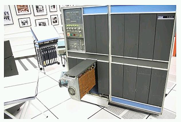
The IBM 1401 mainframe with gate 01B3 opened. This gate contains the arithmetic circuitry,
made up of many SMS cards.
The following block diagram from the 1401 ILD shows the data flow through the adder. The digit from the A register enters on the left, and is translated to qui-binary by the translation circuit (labeled XLATOR). This qui-binary value goes through a translate/complement circuit, which generates the 9's complement value if needed for subtraction. The value in the B register enters on the right and is converted to qui-binary, but without optional complementation. (The IBM 1401 performs operations on memory locations and the A and B registers provide temporary storage for a character read from core. They are not general-purpose registers as in most microprocessors.)
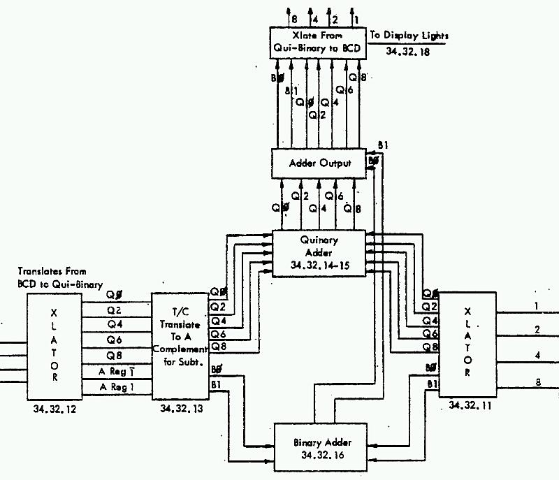
Overview of the arithmetic unit in the IBM 1401 mainframe.
The B0/B1 binary bits and an input carry are added by the binary adder at the bottom. The quinary bits are added with a special quinary adder. The adder output circuit applies any carry from the binary add to the quinary bits, generating the qui-binary result. Finally, a translation circuit converts the qui-binary result to BCD, sending the BCD value to the front panel display and memory. The error checking circuit verifies that the qui-binary has exactly one qui and one binary bit set.
BCD to qui-binary translation
To examine the addition/subtraction circuitry in more detail, we'll start with the logic to convert a BCD digit to qui-binary, as seen below. This diagram is based on page 25 of the ILD.
One surprising feature of the translator is that it accepts binary inputs from 0 to 15, not just "valid" inputs 0 to 9. Input 10 is treated as 0, since the 1401 stores the digit 0 as decimal 10 in core. Values 11 through 15 are treated as 3 through 7. Thus, every binary input results in a valid (but perhaps unexpected) qui-binary value. As a result, the 1401 will perform addition on non-decimal characters.
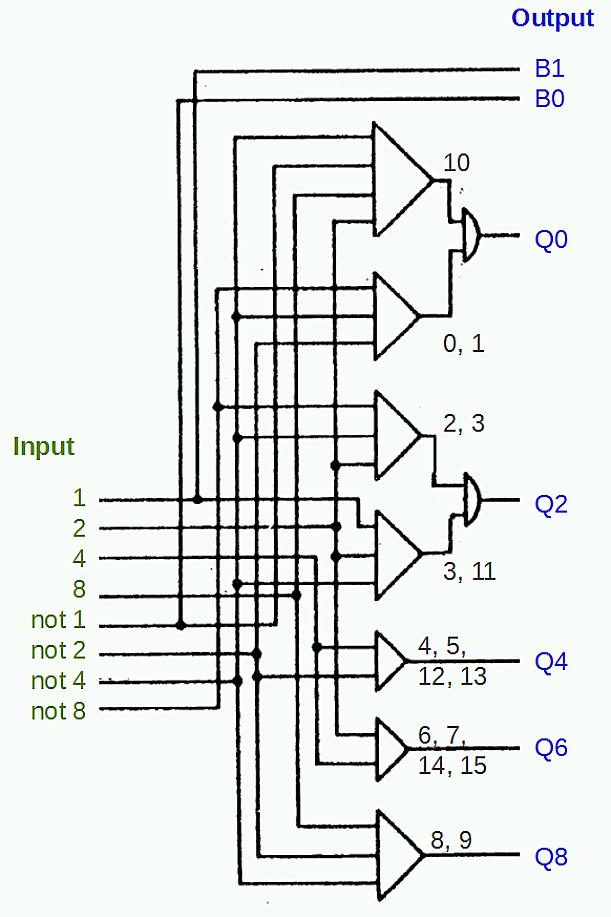
The circuit in an IBM 1401 mainframe to translate a BCD digit into qui-binary code.
The logic is implemented by an AND-OR logic structure that is common in the 1401. Each bit of the BCD digit, as well as each bit's complement, is provided as input. Each AND gate matches a specific bit pattern, and then the results are combined with an OR gate to generate an output.
Note that the logic gate symbols are very different from the modern ANSI standard symbols so don't get them confused. A triangle represents an AND gate, and a semi-circle represents an OR gate.
In qui-binary, the B0 and B1 bits are trivially generated from the low-order binary bit. If the input is even, B0 is set, and if the input is odd, B1 is set.
The first AND gate above matches binary 1010 (decimal 10), and the second AND gate matches binary 000x (decimal 0 or 1). Thus, Q0 will be set for inputs 0, 1, or 10. Likewise, Q2 is set for inputs 2, 3, or 11. The other Q outputs are simpler, computed with a single AND gate.
The translation circuits for the A and B registers are similar, although the A register path also has the complement circuit, which will be described later.
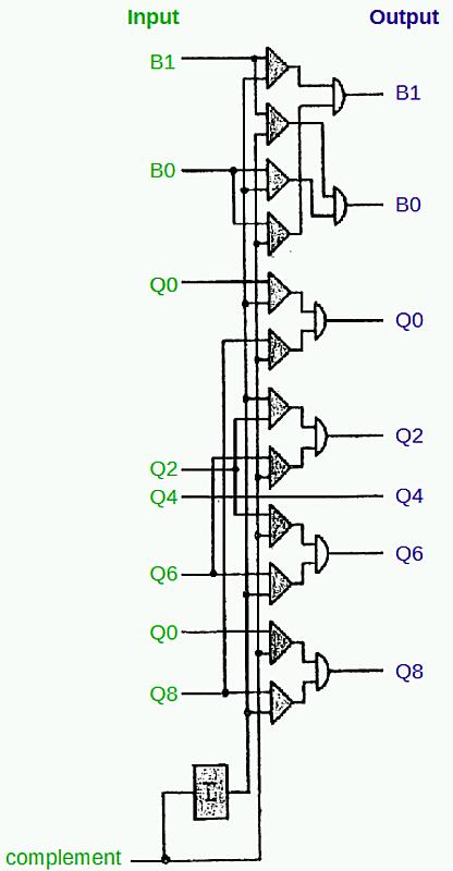
9's complement circuit
The complement circuit is used for subtraction or negative numbers. The circuit generates the 9's complement of a digit, i.e. 9 minus the digit. For example, the 9's complement of 3 is 6, and the complement of 5 is 4. To subtract a number, the 9's complement of each digit is added (along with a carry). For example, consider 432 - 145. The 9's complement of 145 is 854. 432 + 854 + 1 = 1287. Discarding the top digit yields the desired result 287.
To see how complementation works in qui-binary, consider 3 (Q2 B1). Its complement is 6 (Q6 B0). The general pattern for complementation is B0 and B1 get swapped. Q0 and Q8 are swapped, and Q2 and Q6 are swapped. Q4 is unchanged; for example, 4 (Q4 B0) is complemented to 5 (Q4 B1).
The circuit below uses AND-OR logic configured as a multiplexer. For each output, one of two inputs is selected, based on the complement input. (The box labeled I is an inverter.) If complementation is not selected, each input passes through to the output unchanged. This circuit is from page 25 of the ILD. If complementation is selected, the lines are swapped as described earlier. Output B1 comes from input B0, while output B0 comes from input B1. Q0 and Q8 are swapped, and so on.
The complement circuit from the IBM 1401 mainframe. This converts a digit to its 9's complement value.
Quinary adder
The circuit below adds the quinary parts of the two numbers. The qui part of the A register is on the left, the qui part of the B register is on the top, and the qui output is on the right. Each qui result has separate outputs depending if there is a carry or not. An example is Q2 + Q4, shown in red. These two inputs trigger the Q6 output. This circuit is from page 25 of the ILD.
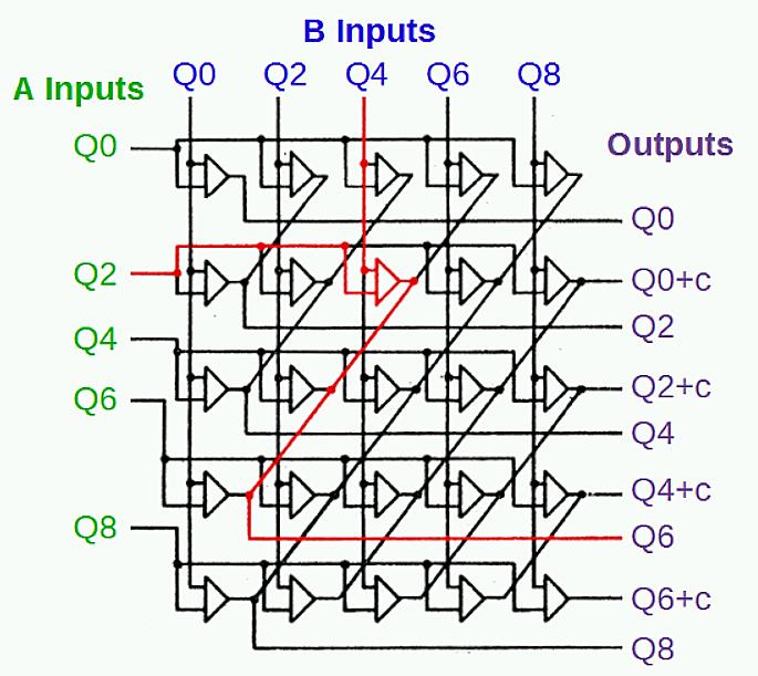
The quinary addition circuit in the IBM 1401 mainframe. This adds the quinary parts
of two qui-binary digits.
The quinary adder is implemented with AND-OR logic, but it uses wired-OR logic. Instead of an explicit gate, the AND outputs are wired together to produce the OR output. While the quinary adder looks symmetrical and regular in the schematic, its implementation uses three different SMS cards: 3JMX and 4JMX AND/OR gates, and JGVW AND gates, depending on the number of AND gates feeding the output.
Qui-binary to BCD output
The diagram below shows the remainder of the qui-binary adder, based on page 26 of the ILD. The qui-binary carry circuit, in the blue box, processes the carry signals from the adder circuit. Using simple OR gates, it generates the qui signals and the qui carry signal. The next circuit, in the green box, applies any carry from the B bits, incrementing the qui component if necessary. For instance, adding 3 + 5 is Q2 B1 + Q4 B1. This generates Q6 + B0 + B carry. The B carry increments the qui component to Q8, yielding the result Q8 B0 (i.e. 8).
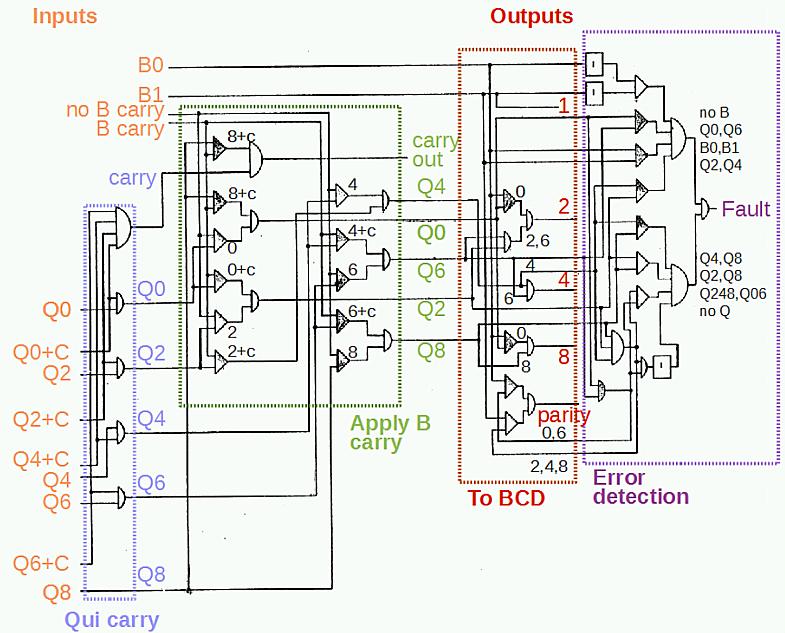
The circuitry in the IBM 1401 mainframe to convert a qui-binary sum to a BCD result.
The translation circuit, in red, converts the qui-binary result to BCD, using straightforward AND-OR logic. Note that 0 is represented in the 1401 as binary 1010, so the 8 and 2 bits are set for Q0 B0.
The parity output is generate by combining the binary parity (even for B0; odd for B1) with the qui parity value. The qui even parity signal is set for Q0 or Q6, while the qui odd parity signal is set for Q2, Q4, Q8. Note that representing 0 as binary 1010 instead of 0000 doesn't affect the parity.
The final circuit, in purple, is the error detection circuit which verifies the qui-binary result is valid. The AND-OR circuit detects a fault if no B bits are set or both B bits are set. Instead of testing every qui bit combination, it implements a short cut from the qui parity circuit. If the even qui parity signal and the odd qui parity signal are both set, this indicates multiple qui lines are set, triggering a fault. If neither qui parity signal is set, then no qui lines are set, also triggering a fault. The parity check misses a few qui combinations (such as Q0 and Q6 set), so these are tested separately. The result is that any invalid qui-binary result triggers a fault.
Conclusion
Addition/subtraction on the 1401 is considerably more complex than the single-digit addition discussed here. First, the signs must be checked to determine if the operation is a true-add or complement-add. Multiple digits are processed until a word mark is encountered. Overflows are counted using the zone adder. A negative result must be recomplemented. Arithmetic on the 1401 and the qui-binary adder are discussed in detail in 1401 Instruction Logic, pages 49-67.
Qui-binary should be distinguished from the more common bi-quinary encoding, where the bi part is 0 or 5, and the quinary part is 0, 1, 2, 3, or 4. Bi-quinary is used in abacuses as well as the IBM 650 and various Univac models. An article by Carl Claunch describes the history leading up to qui-binary arithmetic in detail. A later IBM patent describes qui-binary arithmetic using tunnel diodes: 3308284.